1. Setting up Your Account Environment
Use the ECE teaching server Endeavour at endeavour.ece.iit.edu.
Lab 03 continues directly from Lab 02. Return to the same working directory that contains the Cadence library and files created during Lab 02. Do not create a separate unrelated directory.
cd ~/ece429
source /import/scripts/ece429.cshrc
The command above is the only environment setup command required for the current ECE 429 flow.
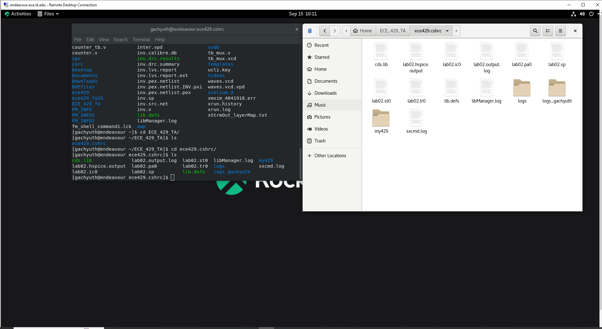
source /import/scripts/ece429.cshrc before launching the CAD tools.Verify that your existing Cadence library, such as my429, is present.
Launch Virtuoso:
virtuoso2. Create the Layout View for the Lab 02 Inverter
In the Library Manager, select the library created in Lab 02, such as my429, and select the inverter cell lab02. The schematic and symbol views should already exist.
- Select library
my429. - Select cell
lab02. - Choose File → New → Cell View.
- Keep the Library and Cell fields as
my429andlab02. - Set the new View to
layout. - Click OK.
lab02 cell so that LVS can compare them later.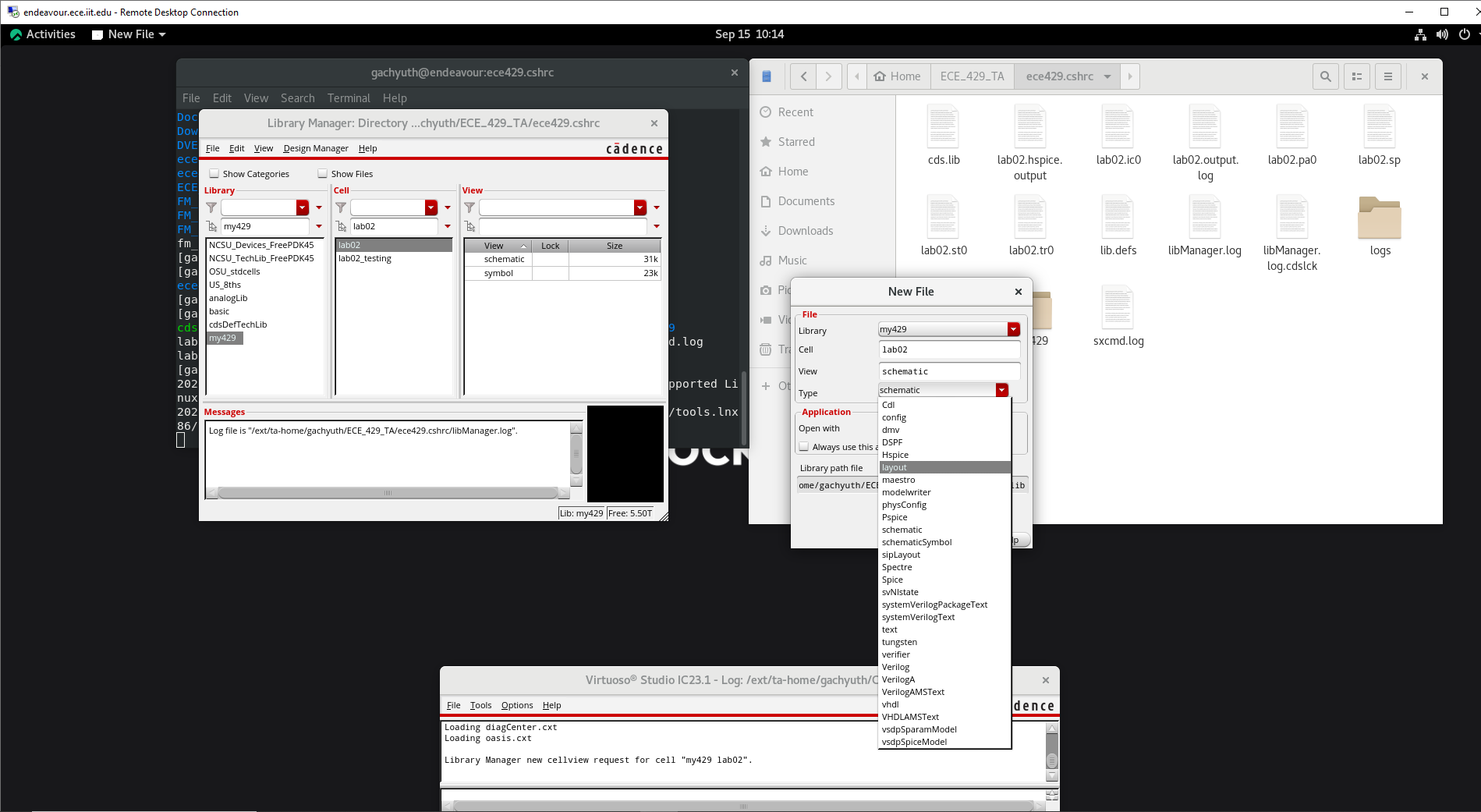
layout view for the existing lab02 cell.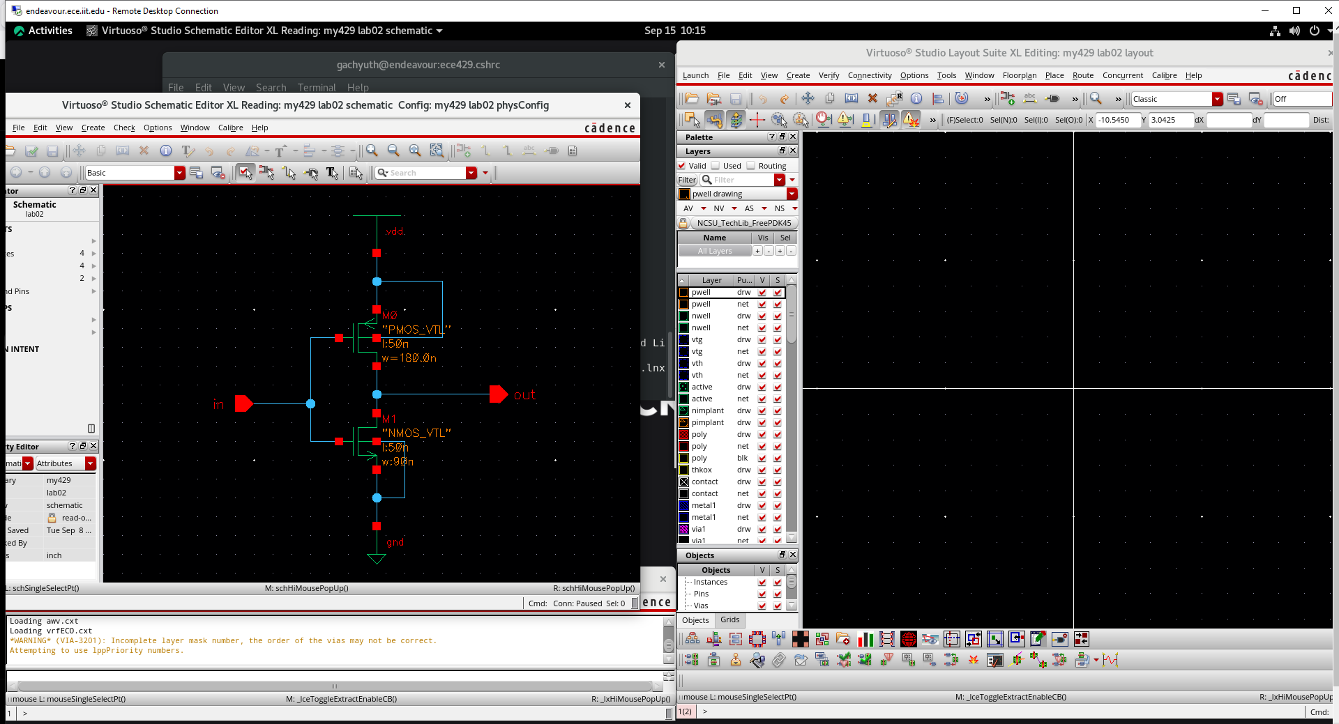
lab02 layout.3. Configure the Layout Grid for FreePDK45
Before drawing anything, configure the grid correctly. This step is compulsory because incorrect snap spacing can produce off-grid or unintended geometry and may cause DRC/LVS problems later.
Choose Options → Display. In Grid Controls, use:
| Setting | Value |
|---|---|
| Type | dots |
| Minor Spacing | 0.01 |
| Major Spacing | 0.1 |
| X Snap Spacing | 0.01 |
| Y Snap Spacing | 0.01 |
The units are micrometers: 0.01 µm = 10 nm and 0.1 µm = 100 nm.
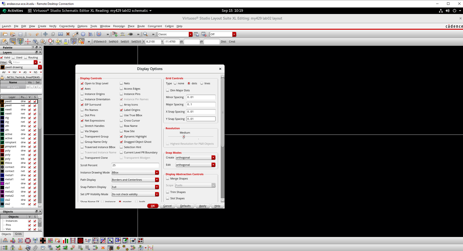
Click OK, press Ctrl+G to refresh/show the grid, and press F to fit the view.
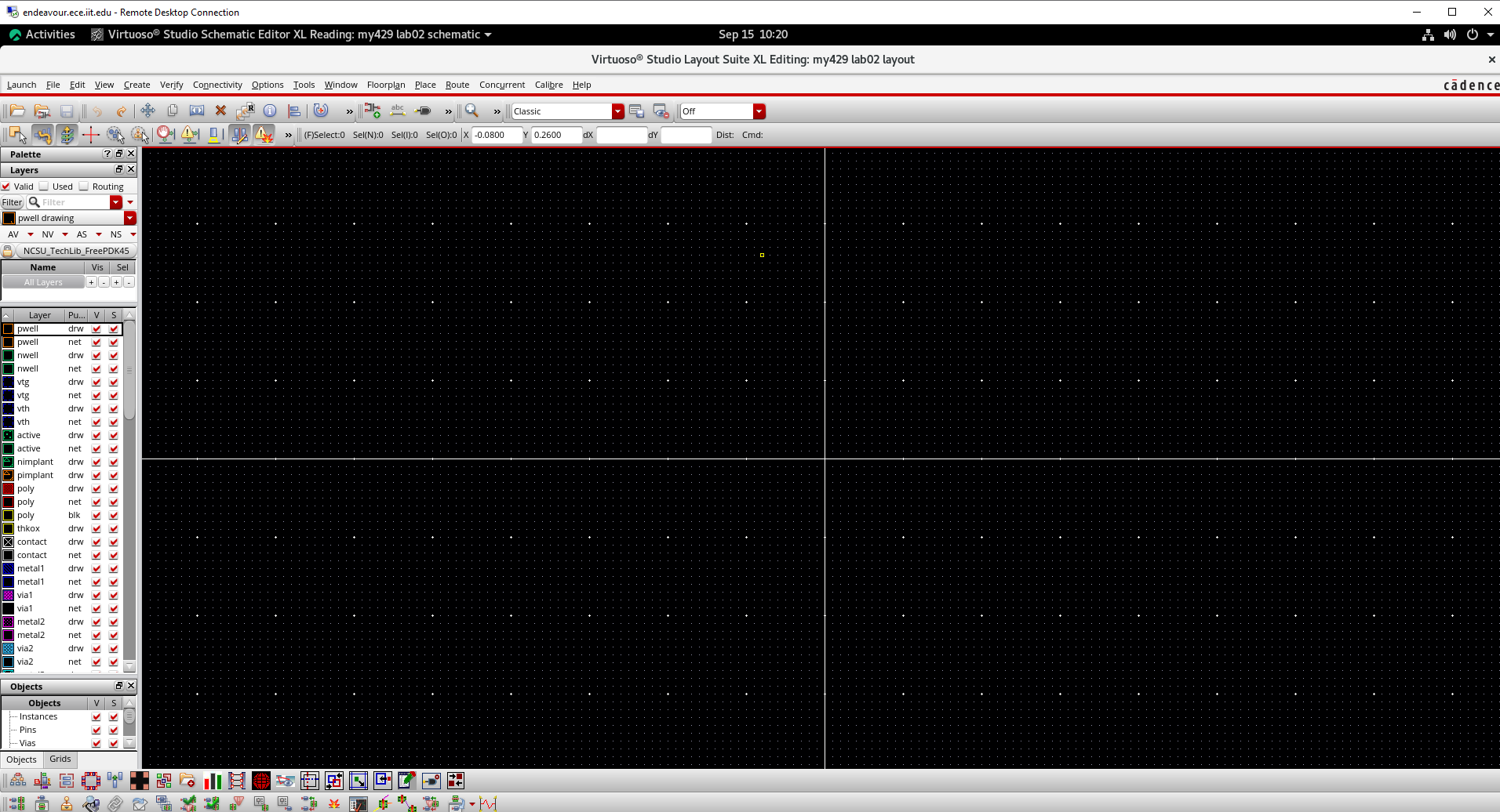
Ctrl+G and fitting the view.4. Reference: Final Inverter Layout
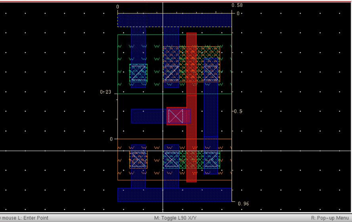
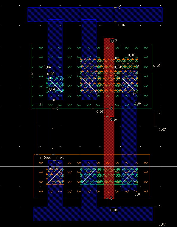
The completed inverter layout is shown below for reference. The PMOS is on top, the NMOS is on the bottom, the gate is shared through polysilicon, VDD is at the top, and GND is at the bottom.
5. Useful Virtuoso Layout Editor Tips
| Action | Shortcut / Method |
|---|---|
| Draw rectangle | Select the layer and press r |
| Measure / ruler | k |
| Move | Select object, then m |
| Copy | Select object, then c |
| Stretch / resize | Select object, then s |
| Zoom in | Ctrl+Z |
| Zoom out | Shift+Z |
| Pan | Arrow keys or mouse wheel |
| Exit active command | Esc |
Press Esc after completing each operation. The active command is also visible through the cursor/status area.
6. NMOS Transistor Layout
6.1 Draw the NMOS Active Region
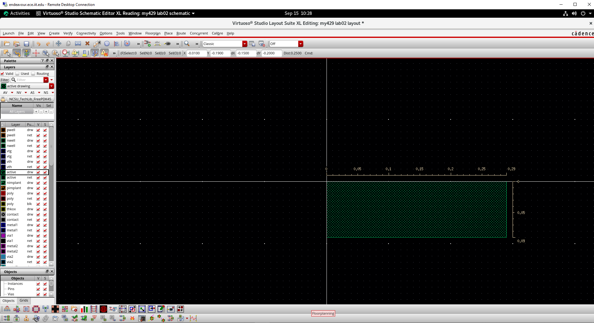
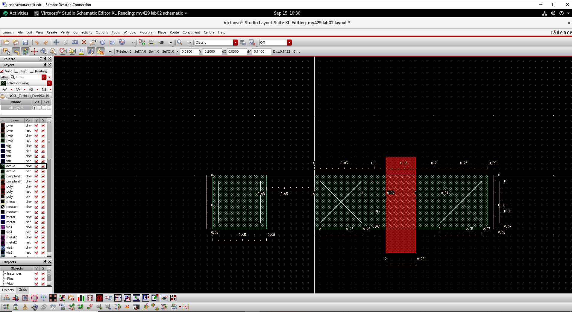
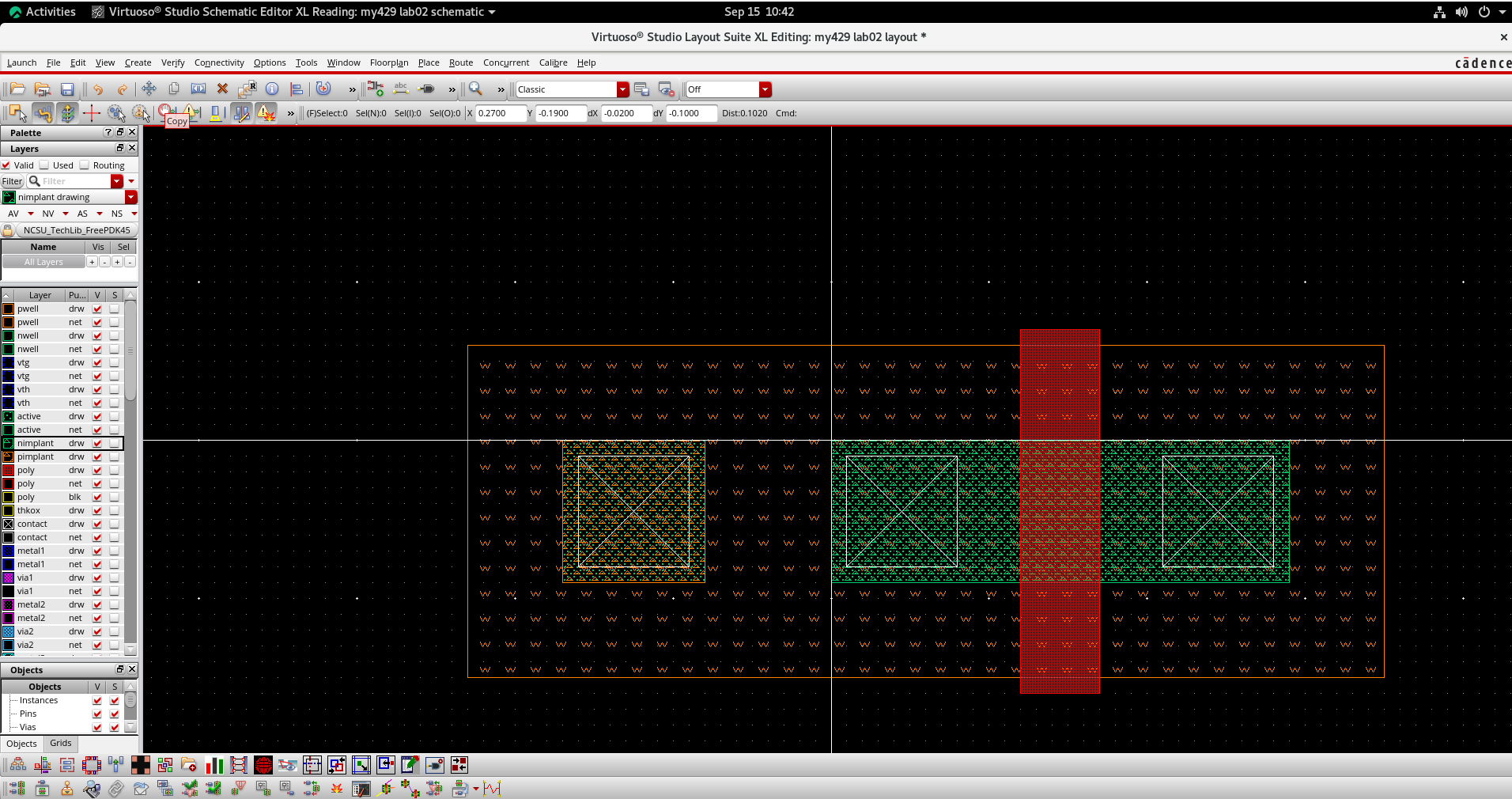
The NMOS has width 90 nm and gate length 50 nm. With a vertical poly gate, the active-region height is 90 nm.
Select active | drw, press r, and draw a 290 nm × 90 nm rectangle. Verify it with k.
6.2 Add Source/Drain Contacts and Poly
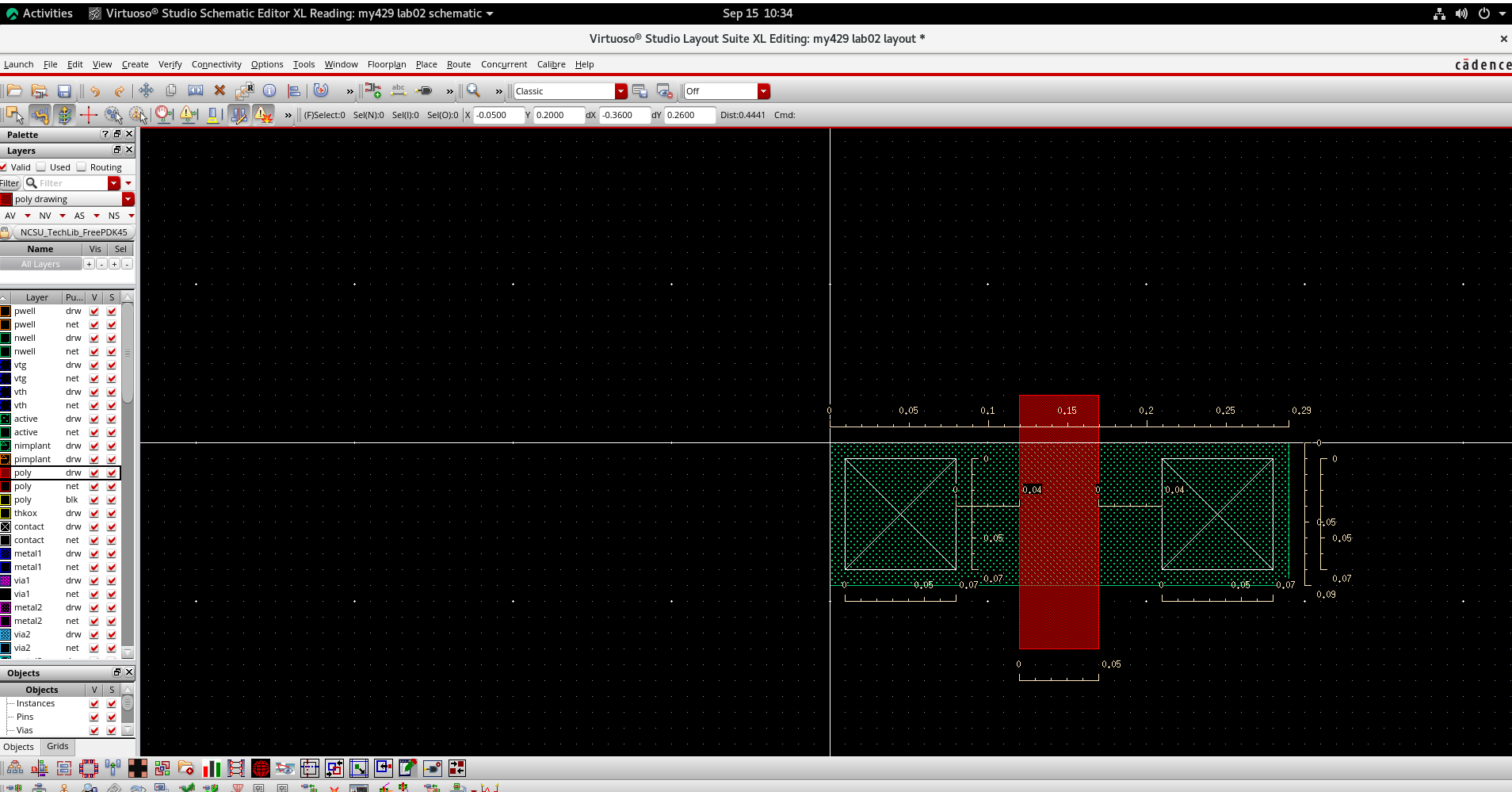
Use contact | drw for two 70 nm × 70 nm contacts. Use approximately 10 nm active enclosure and 40 nm contact-to-poly spacing. Then select poly | drw and draw a vertical 50 nm-wide gate.
Extend the poly at least 60 nm beyond active; this tutorial uses about 70 nm.
6.3 Create the NMOS Body Tap
Create a separate 90 nm × 90 nm active region with a 70 nm × 70 nm contact. Keep approximately 80 nm spacing from the NMOS active region.
6.4 Add the P-Well
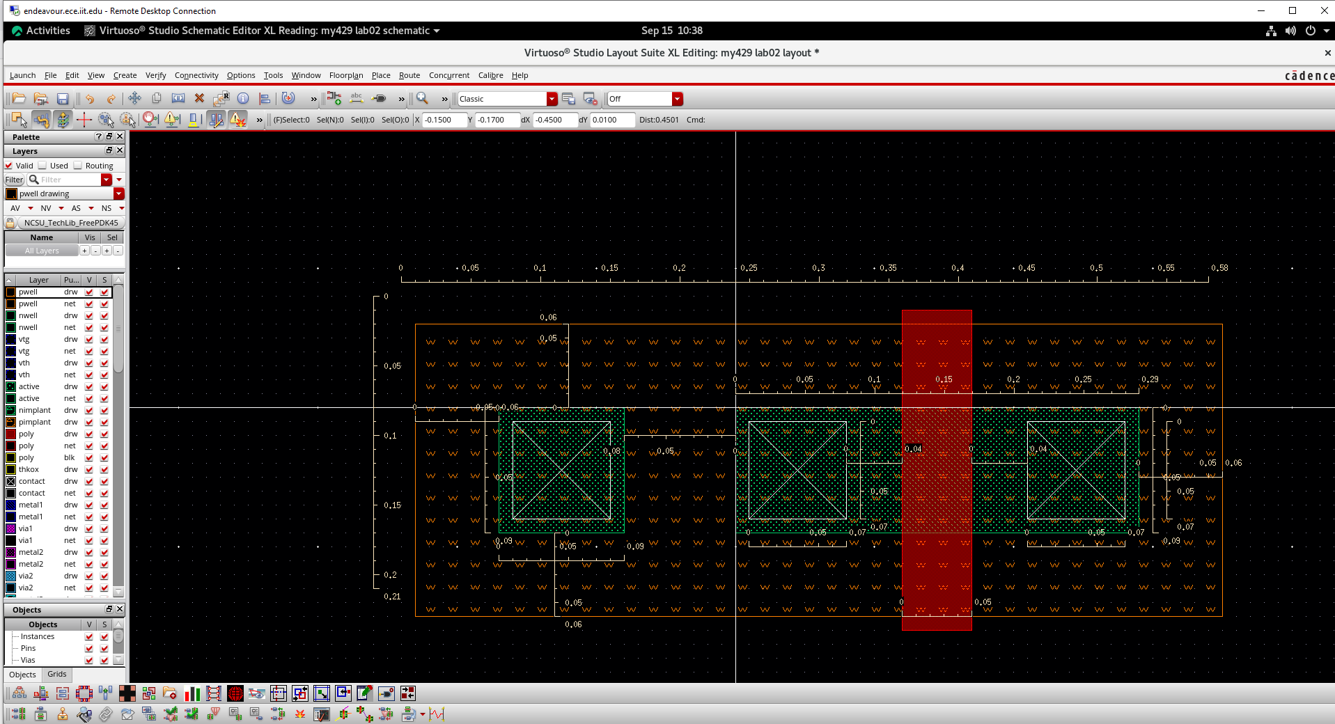
Select pwell | drw and draw a P-well around the transistor and body tap. The tutorial uses approximately 580 nm × 210 nm with about 60 nm active enclosure.
6.5 Add Implant Layers
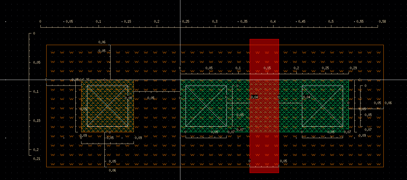
nimplant | drw. The NMOS body tap uses pimplant | drw.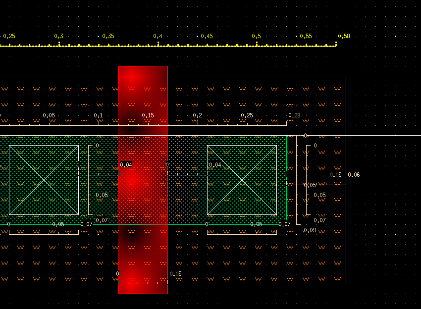
6.6 Clean Up Rulers and Layer Selectability
Remove unnecessary ruler annotations before screenshots. Pay attention to the S (Selectability) column in the layer palette; if a layer is not selectable, you will not be able to move, copy, stretch, or edit its shapes.
6.7 Add Metal1 and GND
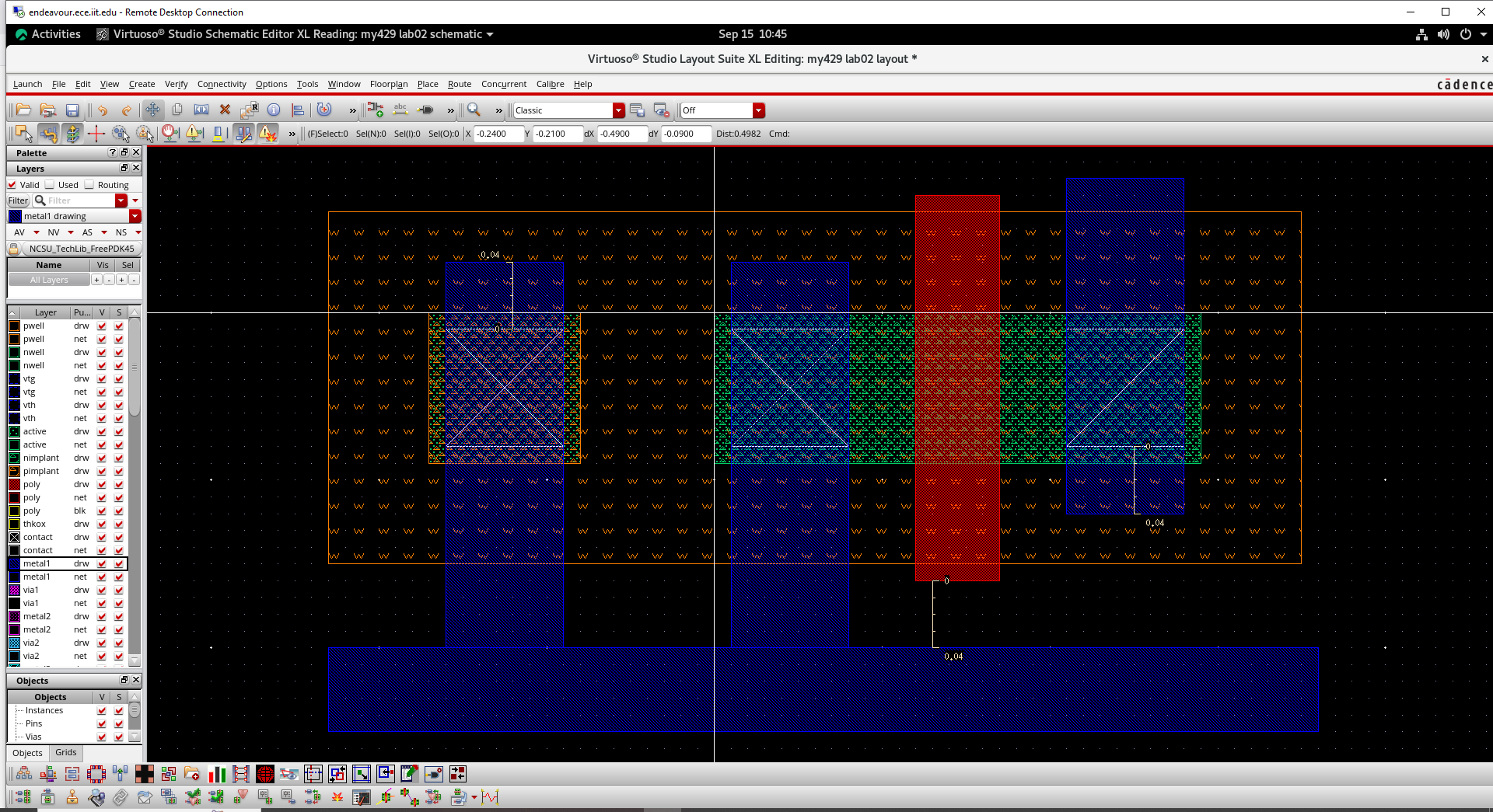
| Metal1 item | Tutorial value |
|---|---|
| Minimum width | 70 nm |
| Minimum spacing | 70 nm |
| Contact enclosure | 40 nm |
Select metal1 | drw, connect the NMOS source/body tap to GND, and draw the GND rail.
7. Design Rule Checking (DRC)
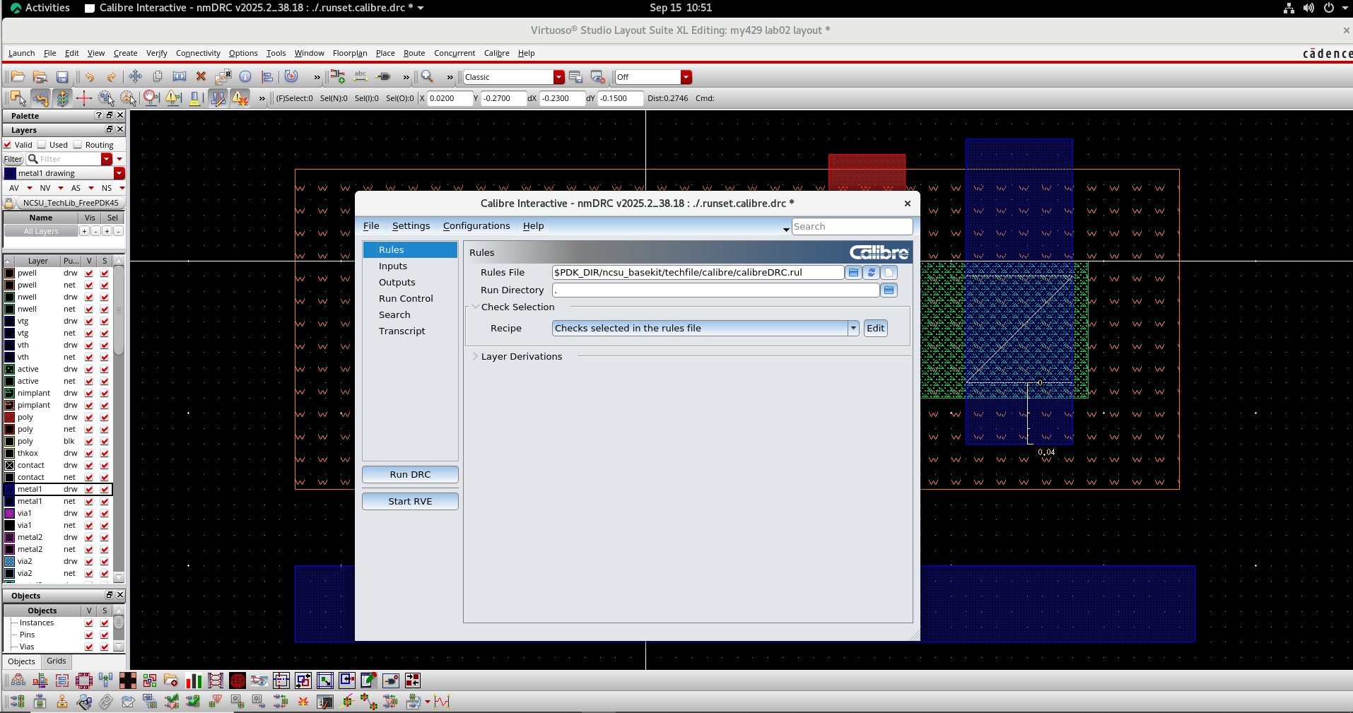
Run DRC frequently while the layout is still simple.
Choose Calibre → Run DRC. The FreePDK45 rule file should already be loaded, normally similar to:
$PDK_DIR/ncsu_basekit/techfile/calibre/calibreDRC.rulClick Run DRC.
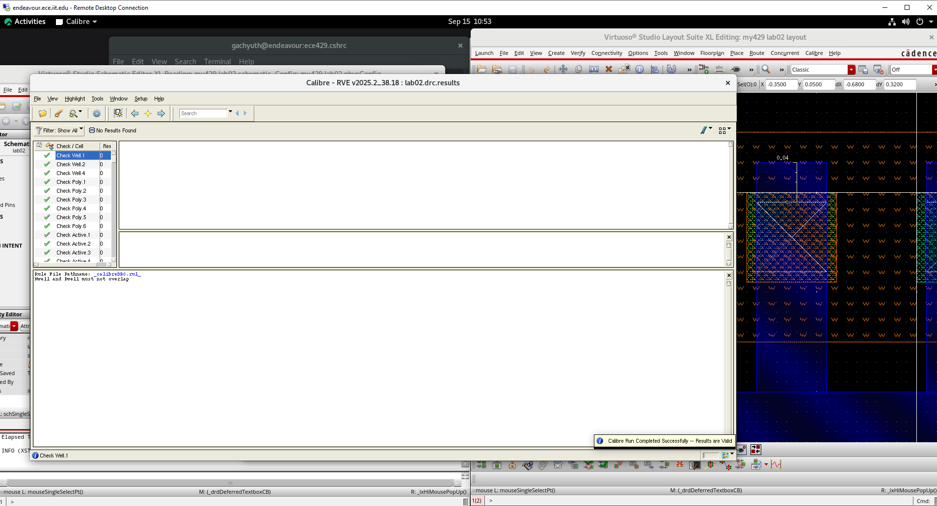
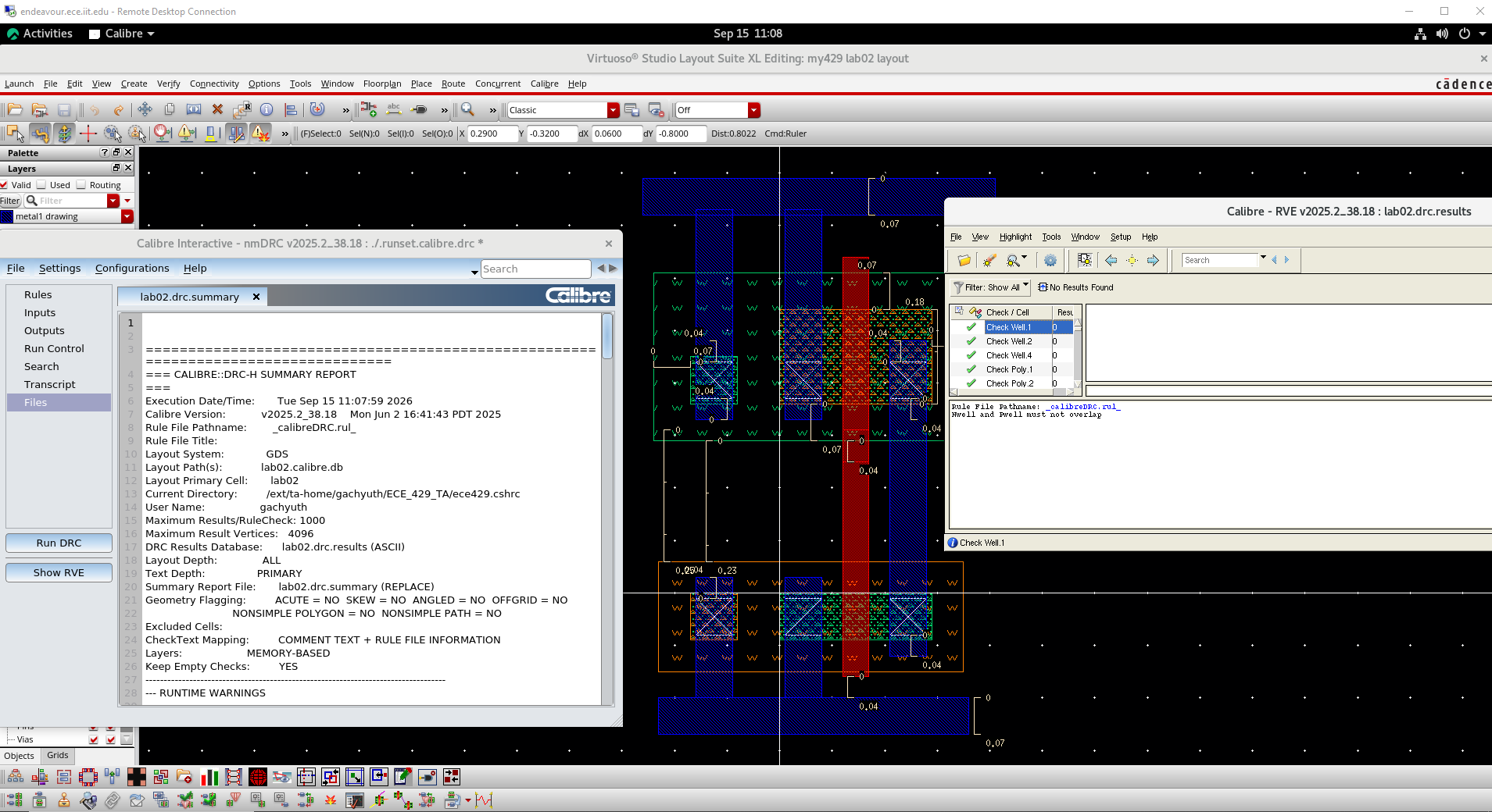
In Calibre RVE, a clean layout shows a result count of 0 for every rule.
8. Create the PMOS Transistor from the NMOS Layout
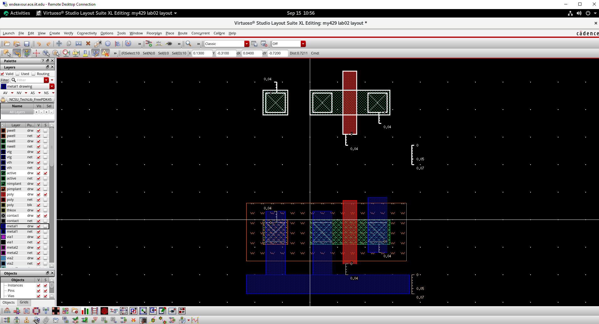
Use the NMOS as a template. Make only the active, contact, and poly layers selectable, box-select those shapes, press c, and place the copy above the NMOS.
8.1 Stretch the PMOS to 180 nm
The PMOS width is 180 nm. Use s to stretch the copied active region from 90 nm to 180 nm and extend the poly as required. Keep the horizontal dimensions unchanged.
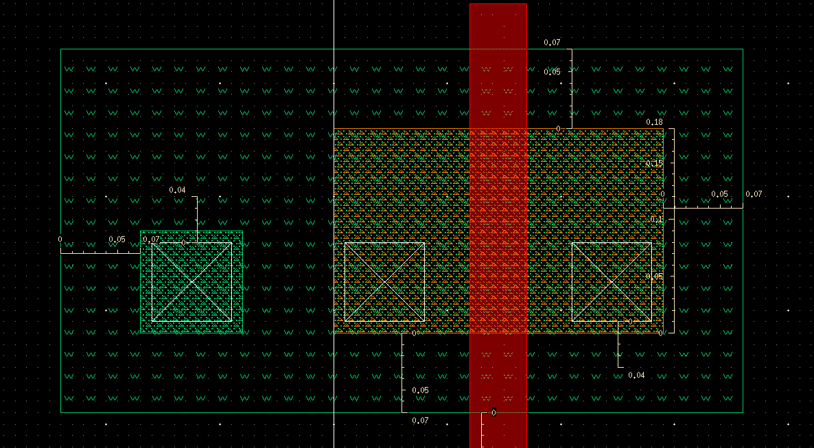
8.2 Add PMOS Implant, N-Well, and Body Tap
pimplant | drw; PMOS body tap uses nimplant | drw; PMOS structures are enclosed by nwell | drw.9. Run DRC Again After Creating the PMOS
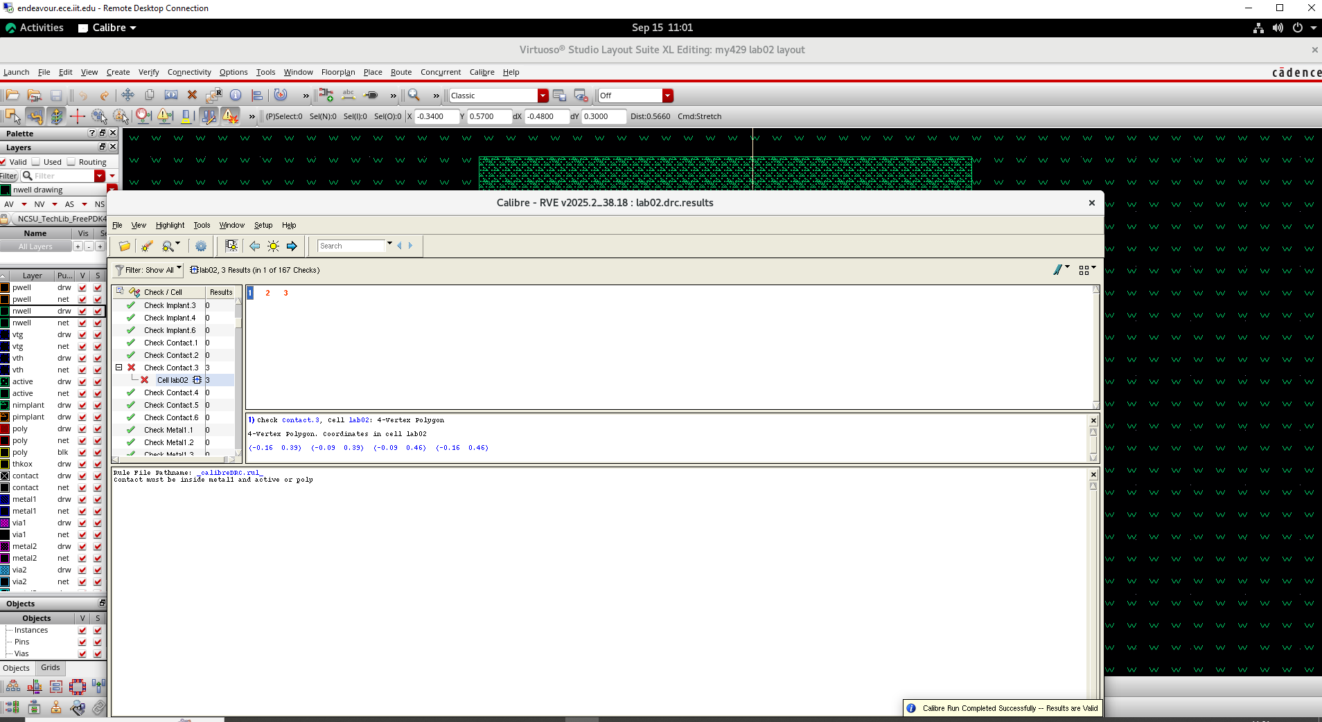
Run Calibre DRC again. If errors appear, expand the failing rule in RVE and use highlight/navigation controls to locate the exact geometry.
In the current example, Calibre reports three Contact.3 violations:
Correct the highlighted geometry and maintain approximately 40 nm Metal1 enclosure around the contact for this tutorial geometry. Rerun DRC until the violations are removed.
10. Complete the Inverter Interconnects
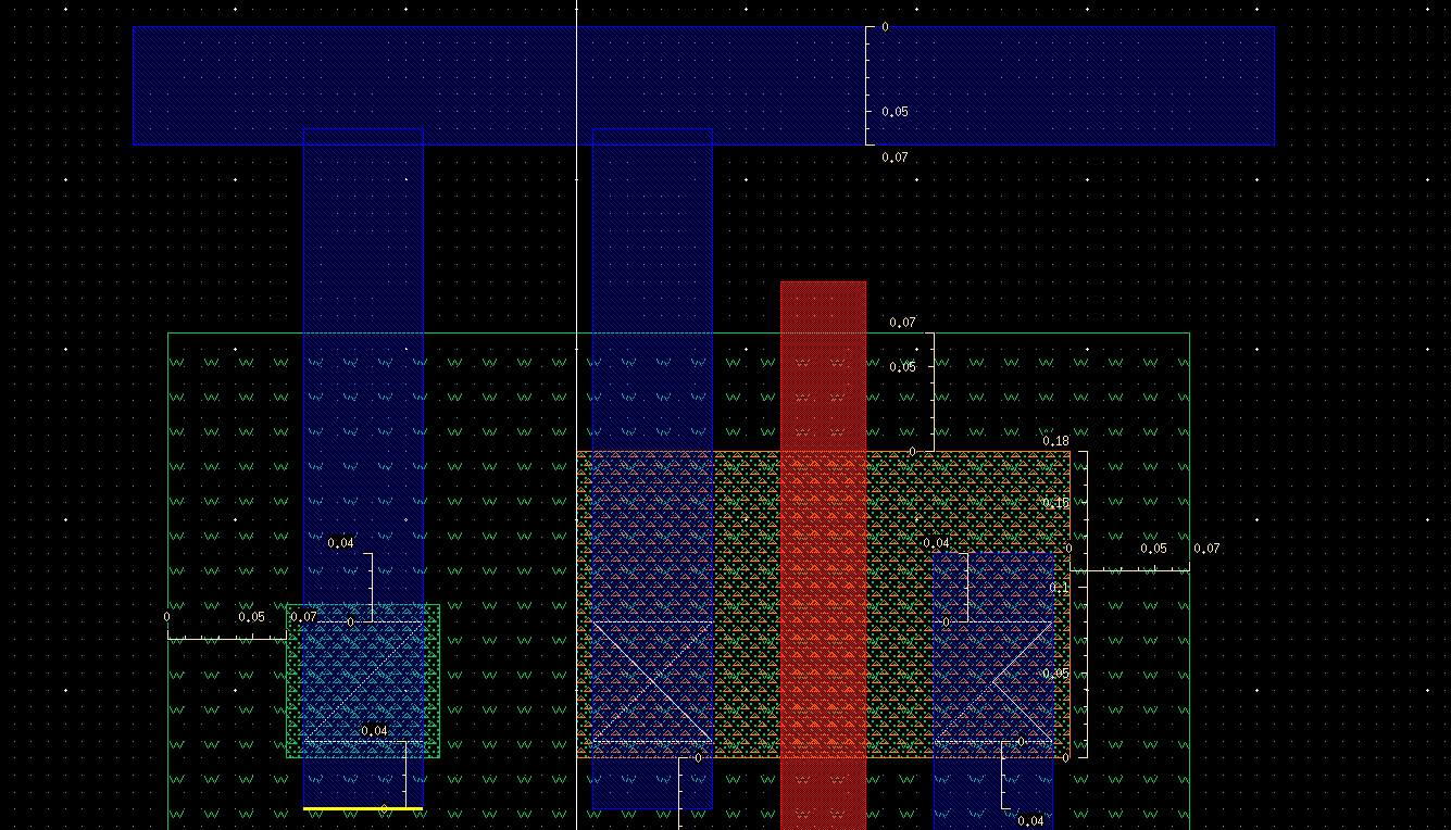
Use metal1 | drw to complete the inverter:
- Create the top VDD rail.
- Connect the PMOS source and body tap to VDD.
- Keep the NMOS source/body tap connected to GND.
- Join the PMOS and NMOS drains to create the output.
- Connect the PMOS and NMOS gates to create the common input.
11. Final DRC Verification
Run Calibre DRC one final time.
12. Layout vs. Schematic (LVS) Verification
DRC checks physical design rules, but it does not prove that the layout is electrically equivalent to the Lab 02 schematic. LVS compares the extracted layout connectivity against the schematic.
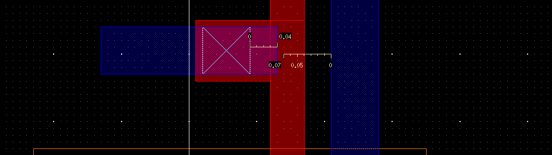
12.1 Complete the Input Metal1 Connection
Before creating pins, connect the common PMOS/NMOS polysilicon gate to Metal1 using the appropriate contact structure so that the inverter input can be accessed as a layout pin.
12.2 Create the Layout Pins
Choose Create → Pin and create these four pins exactly:
vdd!
gnd!
in
out
For each pin, enable Create Label. Click Options and set the label height to approximately 0.05. Use metal1 with purpose drawing.
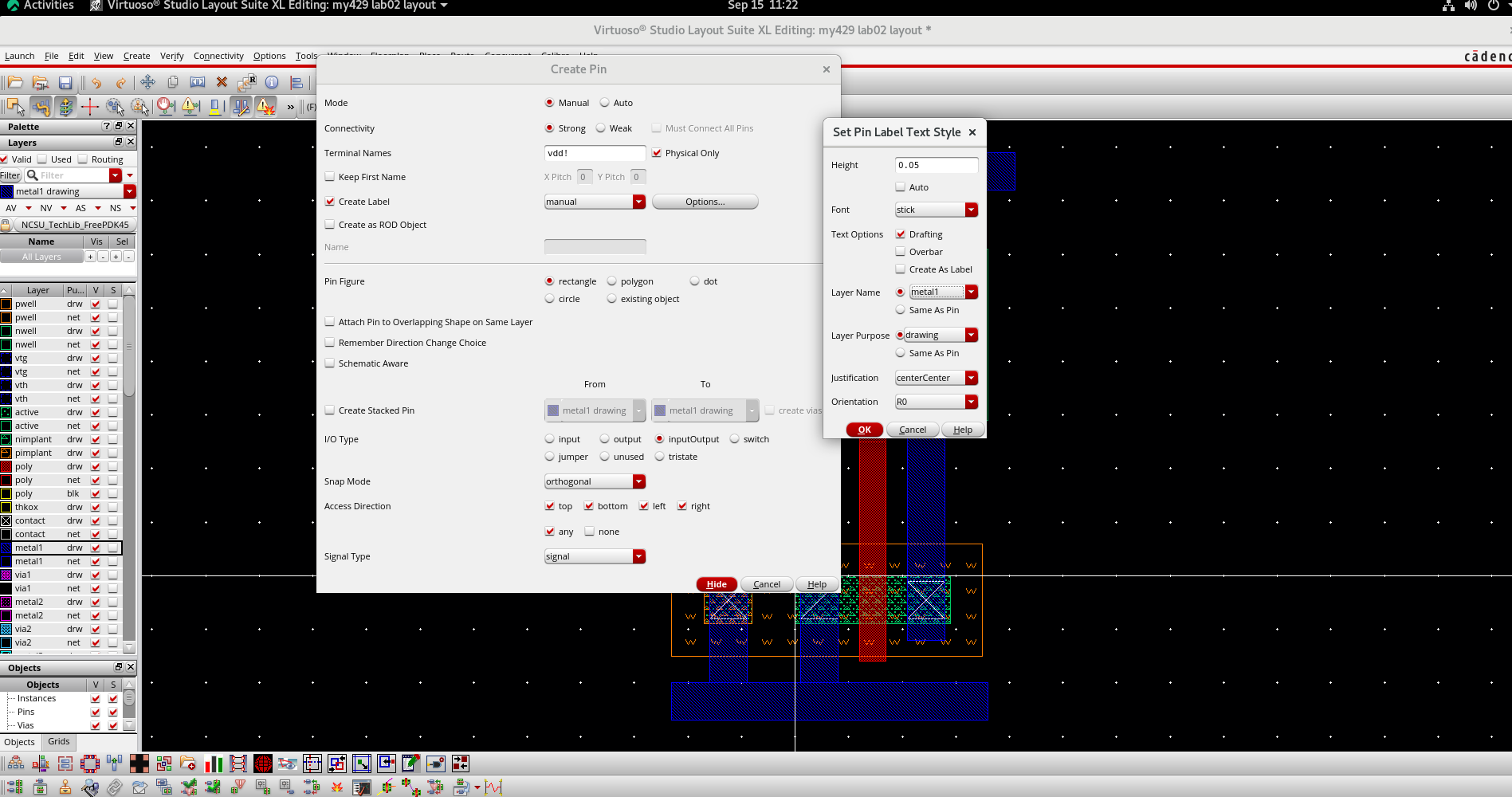
vdd!.| Pin | Place it on |
|---|---|
vdd! | Top VDD Metal1 rail |
gnd! | Bottom GND Metal1 rail |
in | Metal1 connected to the common poly gate |
out | Metal1 connected to the common PMOS/NMOS drain node |
vdd! and gnd!.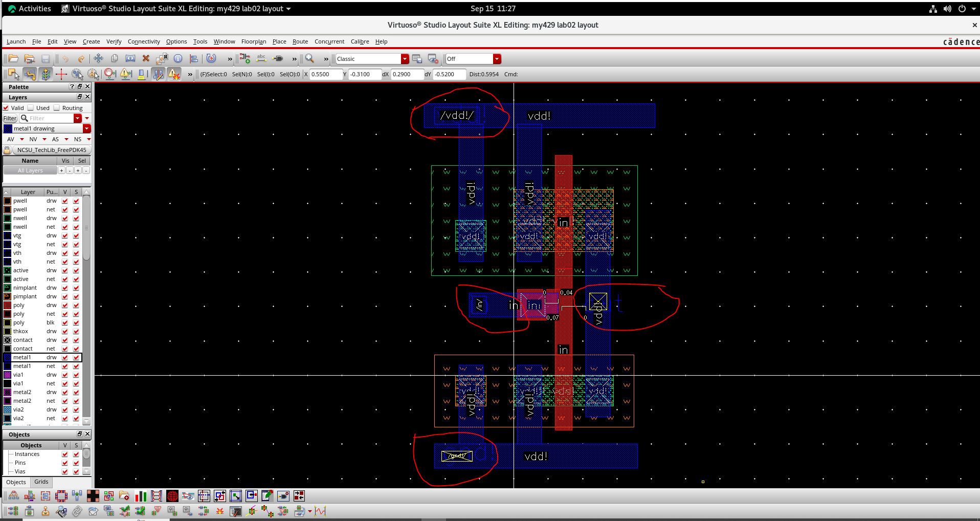
After creating all pins, use File → Check and Save.
13. Run Calibre LVS
Choose Calibre → Run LVS.
In the current Calibre Inputs page, verify both the layout and source in the same window.
| Layout Path | Source Path |
|---|---|
| Layout Format = GDSII | Source Format = SPICE |
| Export from layout viewer = checked | Export from source viewer = checked |
Library = my429 | Library = my429 |
Top Cell = lab02 | Top Cell = lab02 |
View = layout | View = schematic |
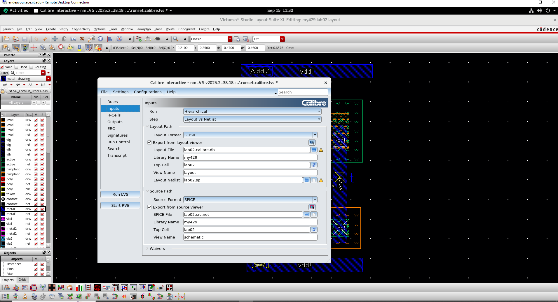
Click Run LVS. A successful result should show:
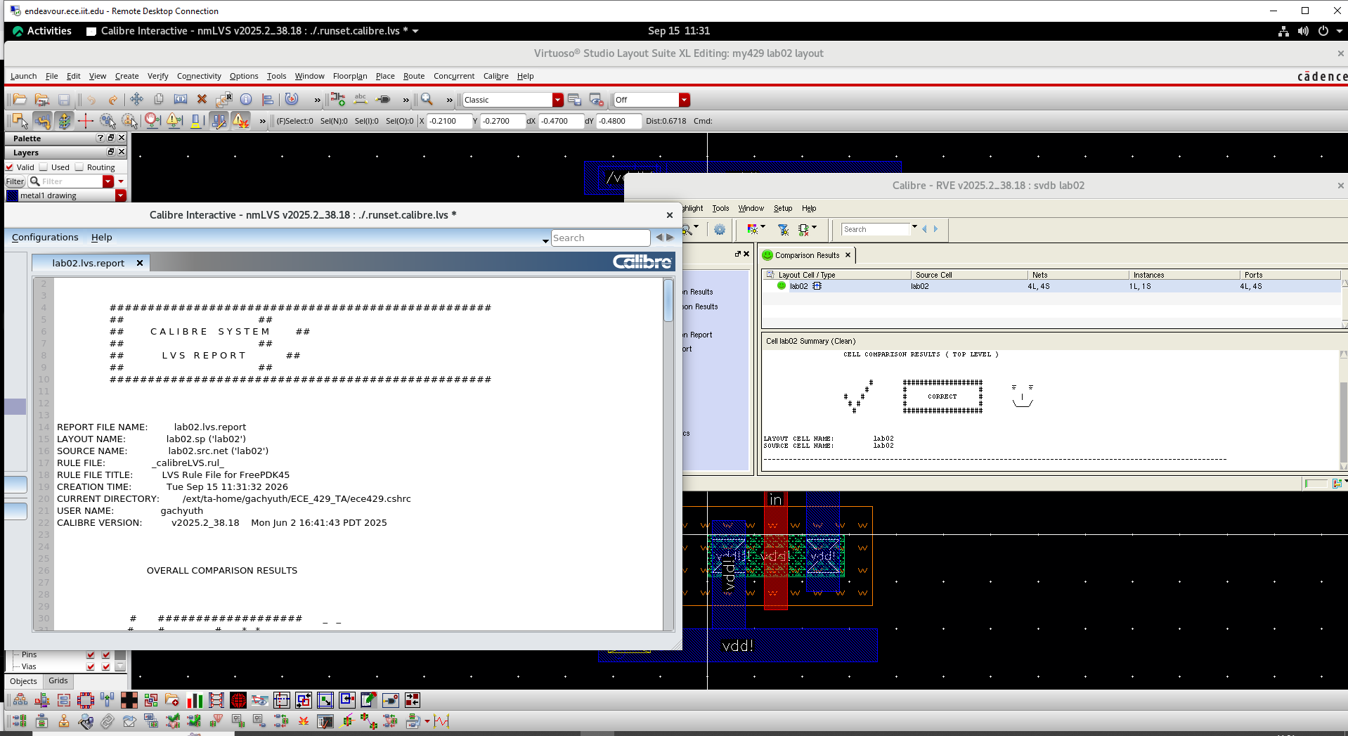
13.1 If LVS Reports an Error
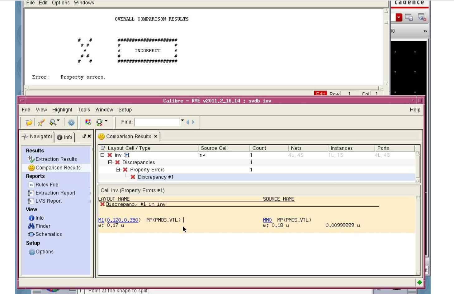
Use Calibre RVE to expand the discrepancy. Common causes include missing/incorrect pins, shorts, opens, wrong body connections, wrong transistor type, or device dimensions that do not match the schematic.
The older screenshot below is included only as an example of how a property mismatch can appear in RVE.
14. Parasitic Extraction and Post-Layout Simulation
Post-layout simulation includes parasitic effects introduced by the physical layout. Calibre PEX extracts these parasitic resistances and capacitances so that HSPICE can simulate a more realistic inverter model.
14.1 Run Calibre PEX
Choose Calibre → Run PEX.
In Inputs, verify:
| Layout Path | Source Path |
|---|---|
| Layout Format = GDSII | Source Format = SPICE |
| Export from layout viewer = checked | Export from source viewer = checked |
Library = my429 | Library = my429 |
Top Cell = lab02 | Top Cell = lab02 |
View = layout | View = schematic |
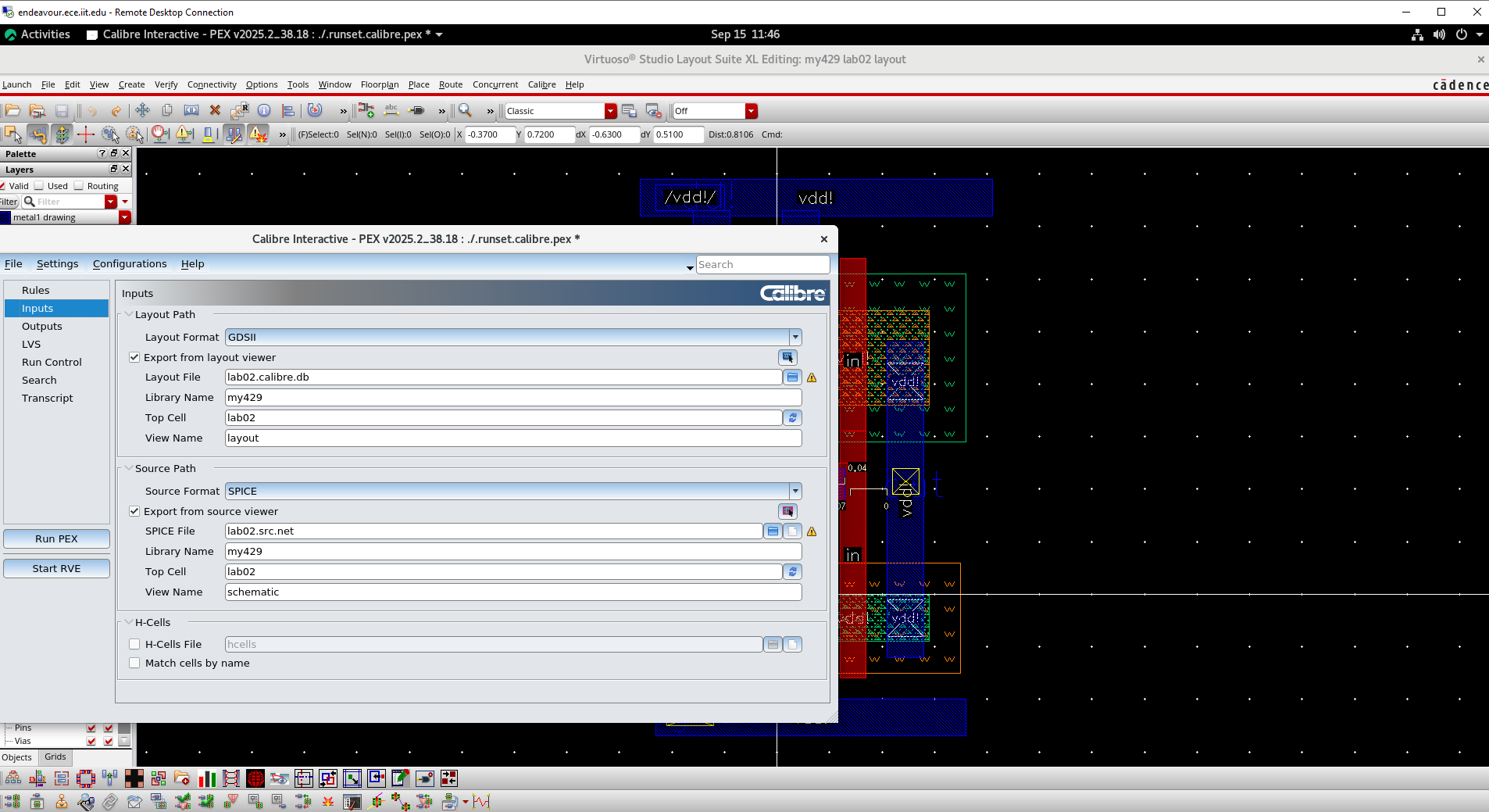
lab02 layout and schematic.14.2 Verify PEX Output Settings
Click Outputs. Leave the current default settings unchanged:
Extraction Mode          = xRC
Level                    = Transistor Level
Resistance/Capacitance   = RCC
Inductance               = No Inductance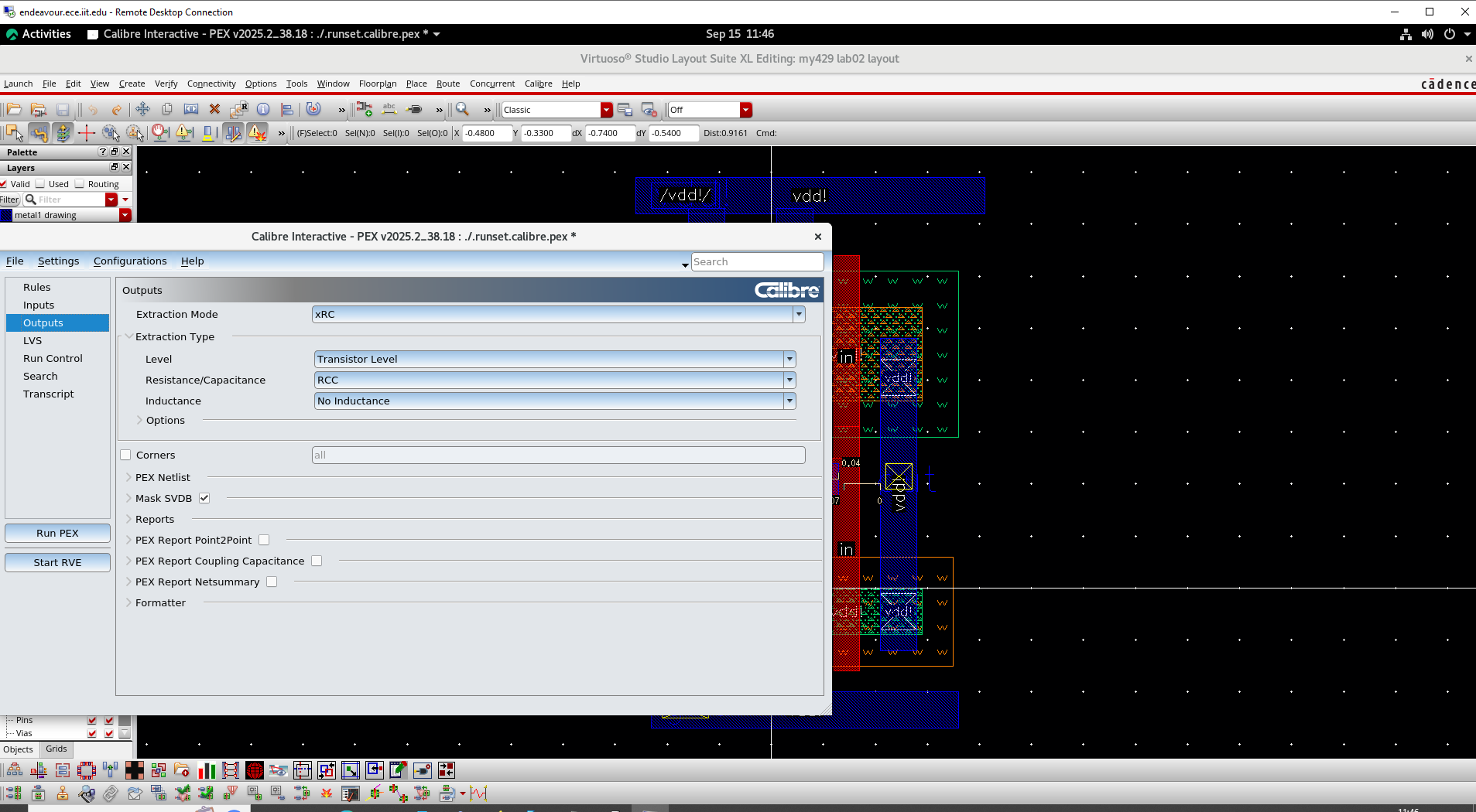
14.3 Run PEX
Click Run PEX. The current flow does not require a separate extracted-layout window to appear. Verify the transcript.
A successful run should show:
xRC Errors = 0
xRC run finished with exit code 0
Warnings may be present. For this lab, the required condition is zero xRC errors.
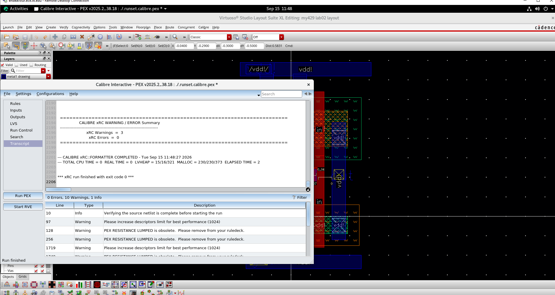
Save your work and close Virtuoso. Keep a terminal open in the same ECE 429 working directory.
14.5 Post-Layout Simulation with HSPICE
14.5.1 Locate the Extracted Netlist
After PEX, the working directory should contain the extracted parasitic netlist:
lab02.pex.netlistThe original Lab 02 simulation file lab02.sp should also still be present.
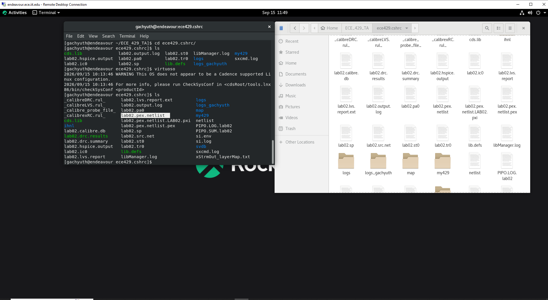
lab02.pex.netlist and the Lab 02 simulation files.14.5.2 Create the Lab 03 SPICE File
cp lab02.sp lab03.sp
gedit lab03.sp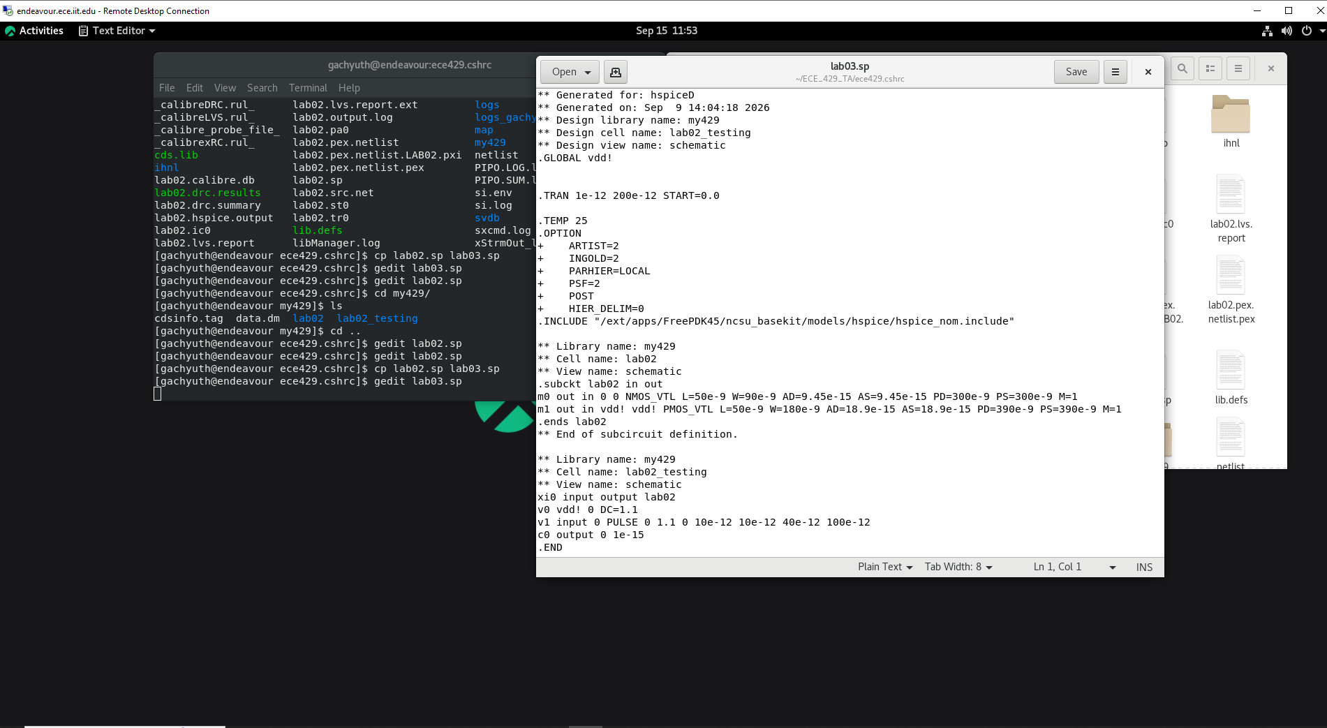
lab03.sp from the Lab 02 HSPICE simulation file.14.6 Replace the Schematic Subcircuit
In lab03.sp, comment out every line of the original schematic subcircuit from .subckt lab02 ... through .ends lab02 by adding * at the beginning of each line.
*.subckt lab02 in out
*m0 ...
*m1 ...
*.ends lab02

.INCLUDE "lab02.pex.netlist"
14.7 Verify the Extracted Pin Order
Open lab02.pex.netlist and find the extracted subcircuit declaration. In the current extraction it is:
.SUBCKT LAB02 IN GND! VDD! OUTThe instance in lab03.sp must use this exact terminal order.
14.8 Update the Inverter Instance
Replace the original schematic instance:
xi0 input output lab02with:
xi0 input gnd! vdd! output lab02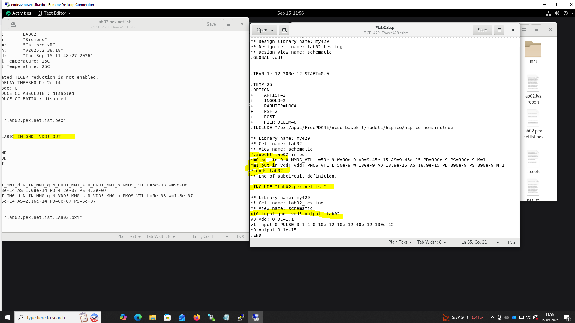
lab03.sp accordingly.lab03.sp must exactly match the .SUBCKT order in lab02.pex.netlist.14.9 Run the Post-Layout HSPICE Simulation
hspice lab03.sp | tee lab03.hspice.output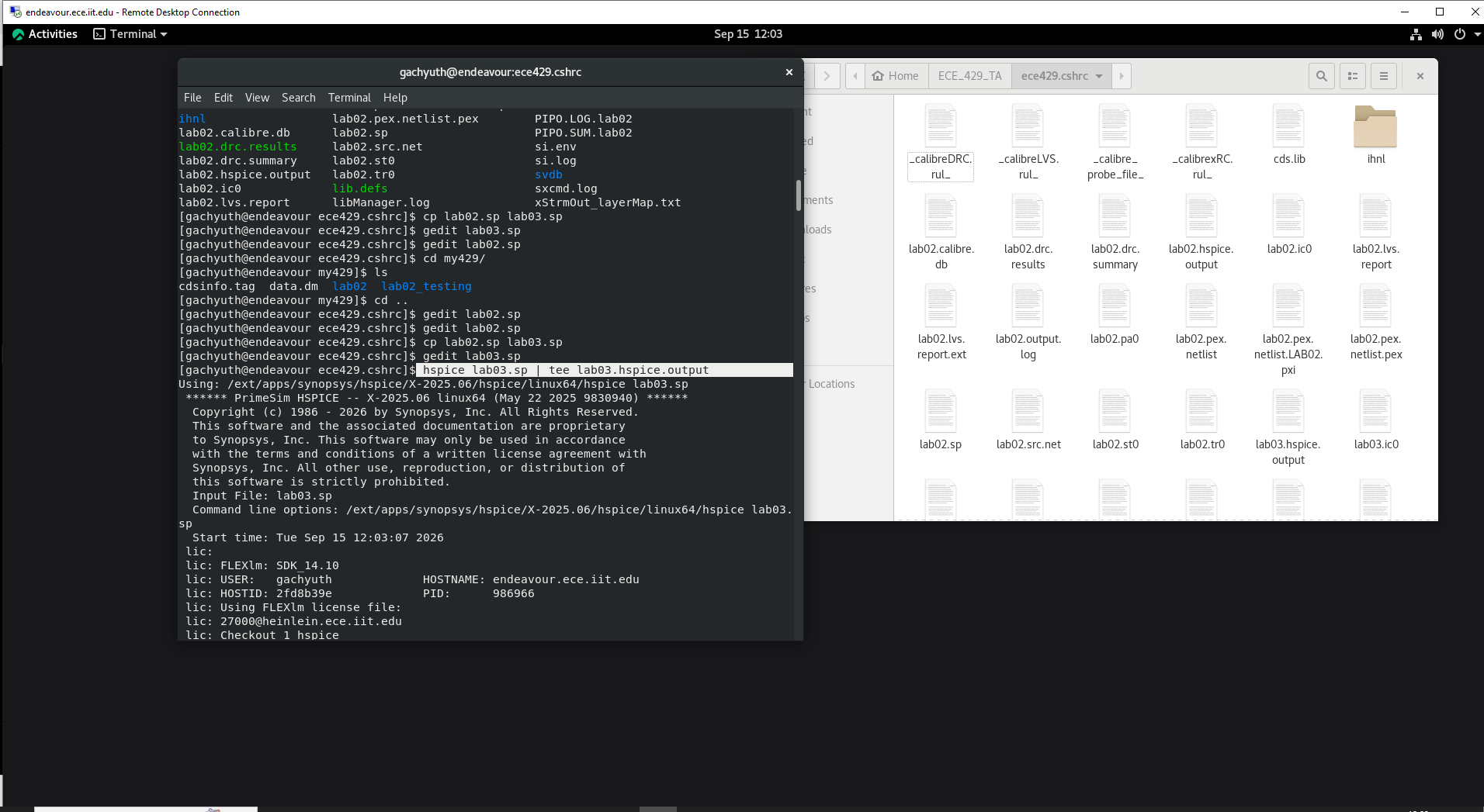
lab03.sp.A successful run ends with:
hspice job concluded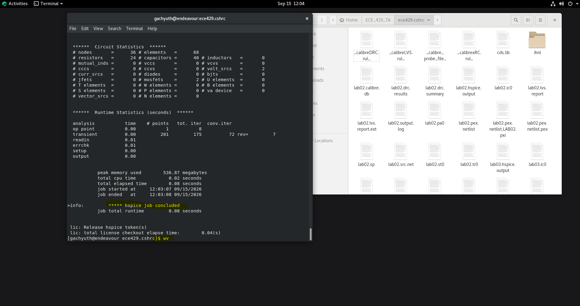
hspice job concluded.14.10 View the Post-Layout Waveforms and Measure Delay
Launch Synopsys WaveView:
wvOpen lab03.tr0, expand the top-level signals, and display:
v(input)
v(output)
14.11 Measure Post-Layout Propagation Delay
Use Measurement Tool → Time Domain → Delay. Set:
Signal      = v(output)
Ref. Signal = v(input)
Measurement level = 50%
For a 0–1.1 V logic swing, the 50% crossing is 0.55 V.
| Delay | Output transition | Input reference |
|---|---|---|
| tPHL | High → Low | Low → High |
| tPLH | Low → High | High → Low |
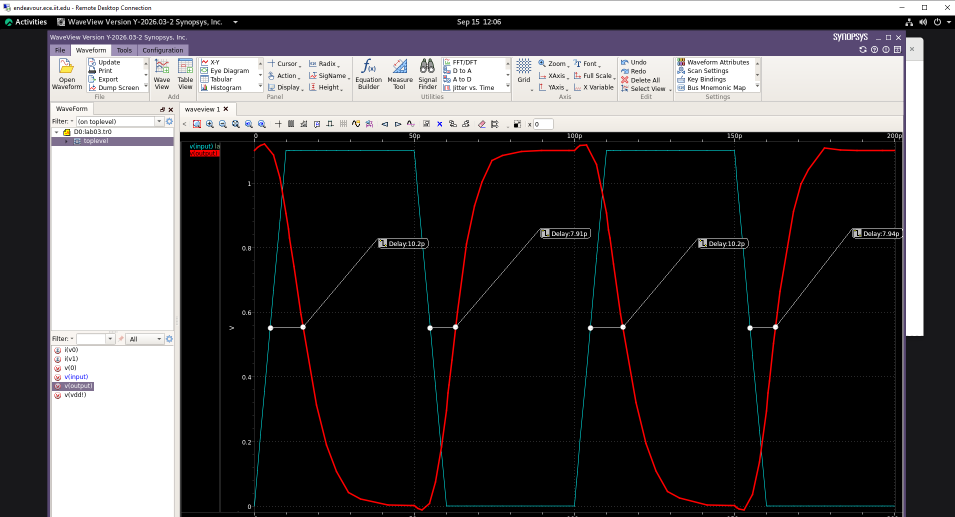
14.12 Compare Schematic and Post-Layout Delay
| Simulation | tPHL | tPLH | tpd |
|---|---|---|---|
| Lab 02 schematic | Your value | Your value | Your value |
| Lab 03 post-layout | Your value | Your value | Your value |
The post-layout delay generally differs from the schematic-only delay because the PEX model includes physical interconnect/device parasitic resistance and capacitance.
- Completed inverter layout.
- Final DRC result with 0 violations.
- LVS result showing CORRECT.
- PEX result showing 0 xRC errors.
- Successful HSPICE run ending with
hspice job concluded. - WaveView plot showing
v(input),v(output), and post-layout delay measurements. - Schematic-vs-post-layout delay comparison.