Overview
This tutorial introduces the Cadence Virtuoso custom IC design environment. You will create a CMOS inverter schematic, generate a reusable symbol, build a testbench, export an HSPICE netlist, run a transient simulation, and inspect the results in Synopsys WaveView.
1. Setting up Your Account Environment
Use the ECE teaching server Endeavour (endeavour.ece.iit.edu), which runs Rocky Linux.
Open a terminal
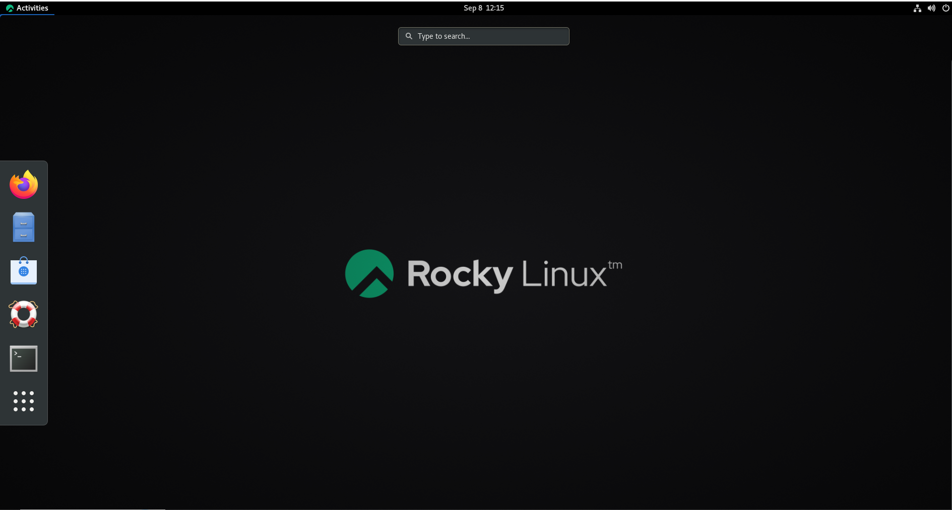
- Click Activities in the upper-left corner of the Rocky Linux desktop.
- Open Terminal from the applications menu or search for “Terminal.”
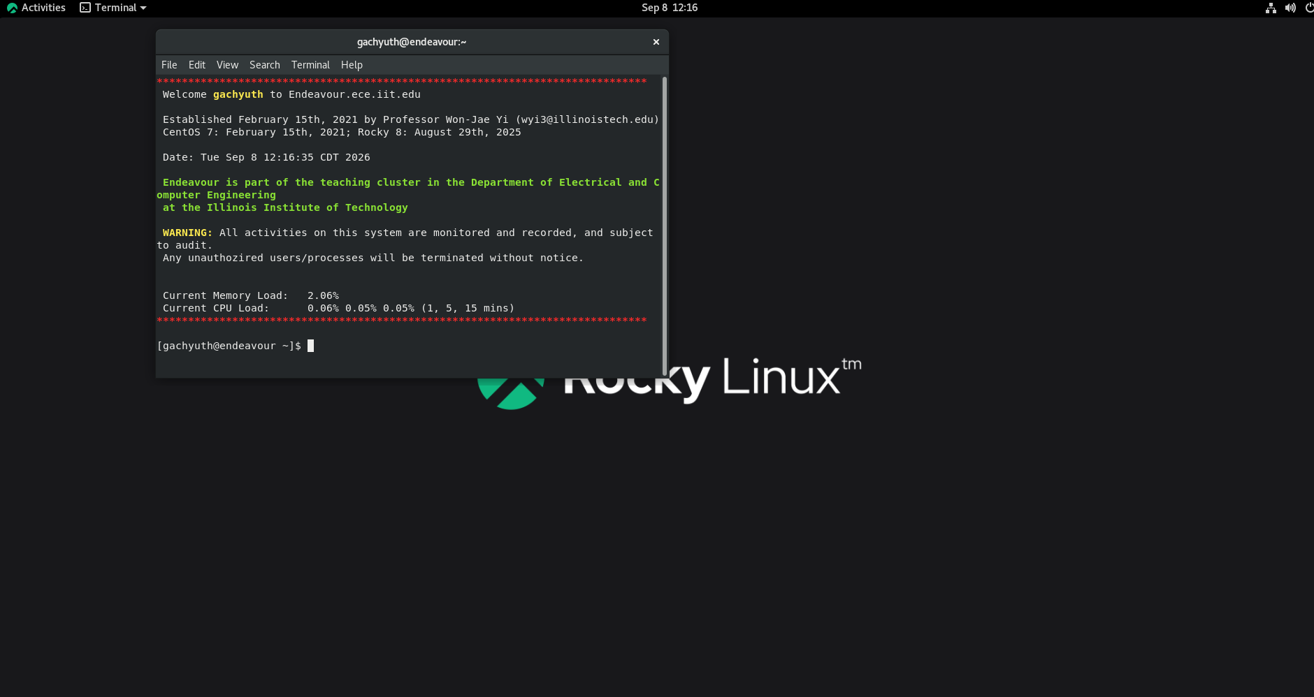
- Confirm that the prompt shows your Endeavour account.
Create the ECE 429 working directory and load the environment
Create one working directory in your home directory and enter it:
mkdir ~/ece429
cd ~/ece429
Load the course environment:
source /import/scripts/ece429.cshrcAfter the setup completes, files such as cds.lib and lib.defs should be present in the working directory.
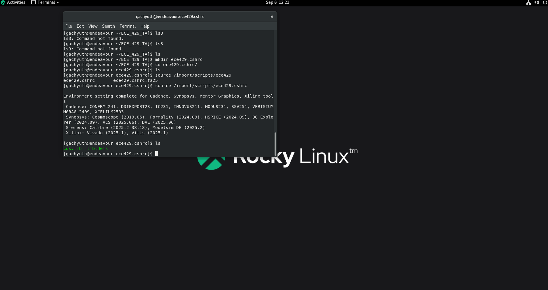
~/ece429 and run source /import/scripts/ece429.cshrc before launching the design tools.2. Inverter Schematic Using Virtuoso
2.1 Start Virtuoso
From ~/ece429, launch Virtuoso:
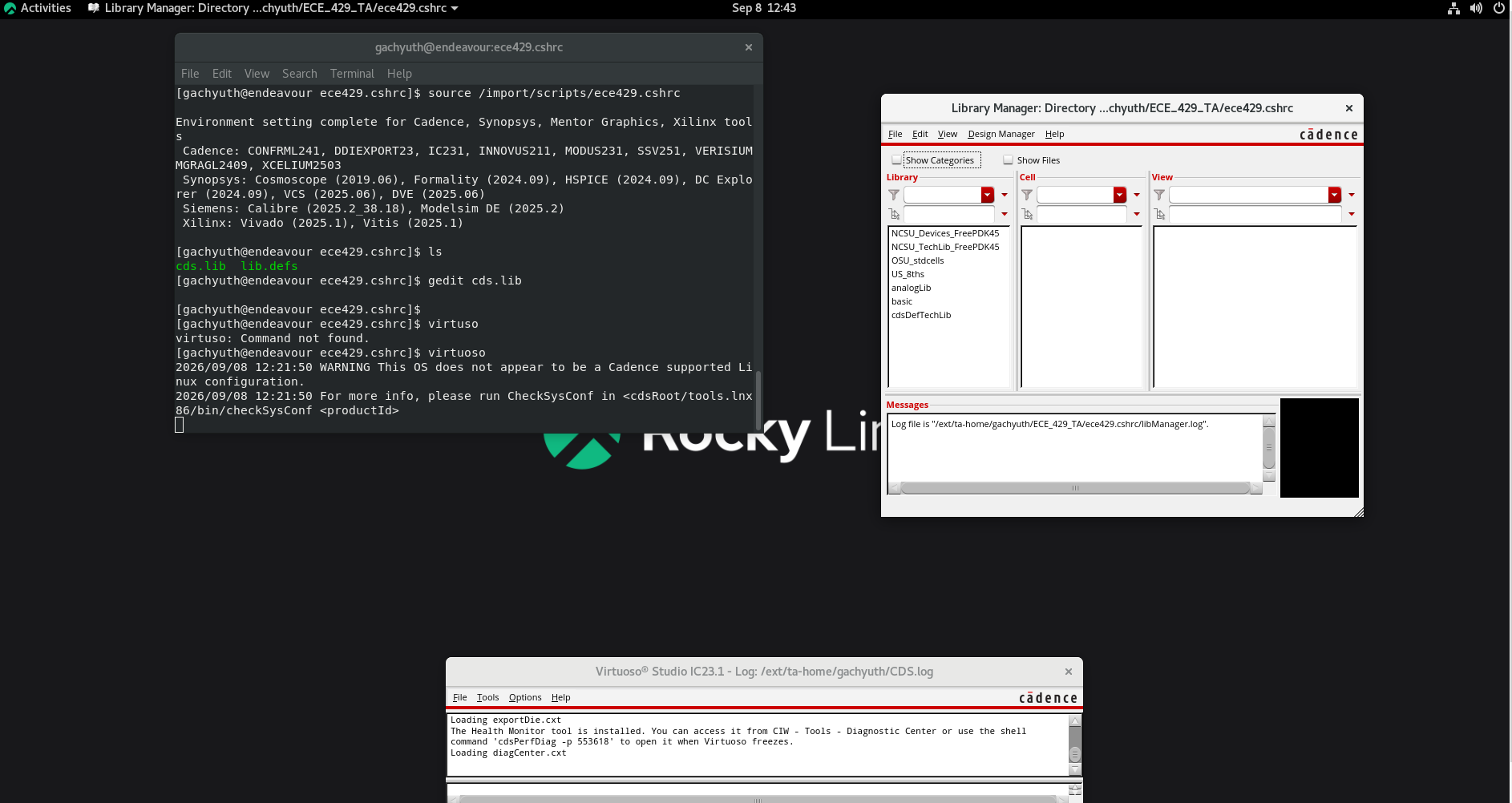
virtuosoVirtuoso Studio and the Library Manager should open. Verify that the FreePDK45 libraries are visible, including NCSU_Devices_FreePDK45 and NCSU_TechLib_FreePDK45.
2.2 Create your design library
- In Library Manager, choose File → New → Library.
- Set the library name to
my429. Keep the directory in your current ECE 429 working directory, then click OK. - In Technology File for New Library, choose Attach to an existing technology library and click OK.
- Select
NCSU_TechLib_FreePDK45and click OK.
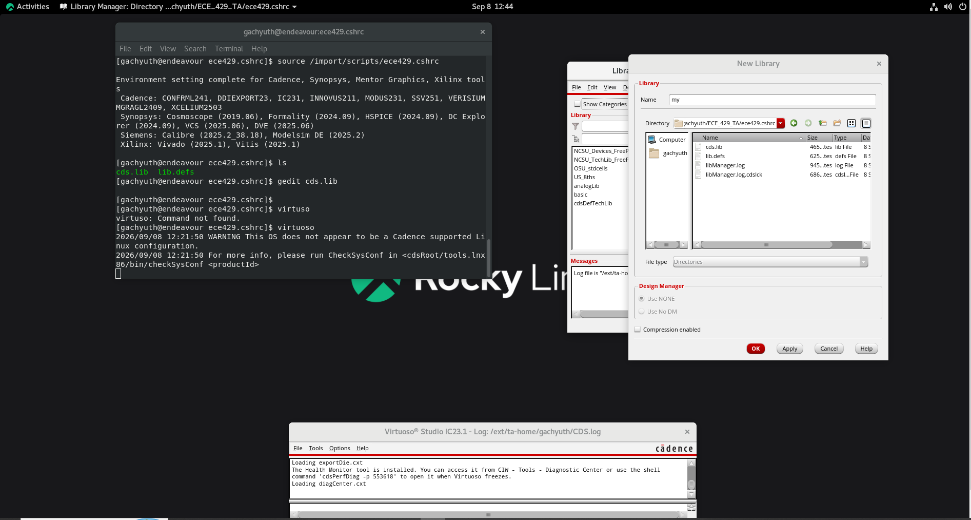
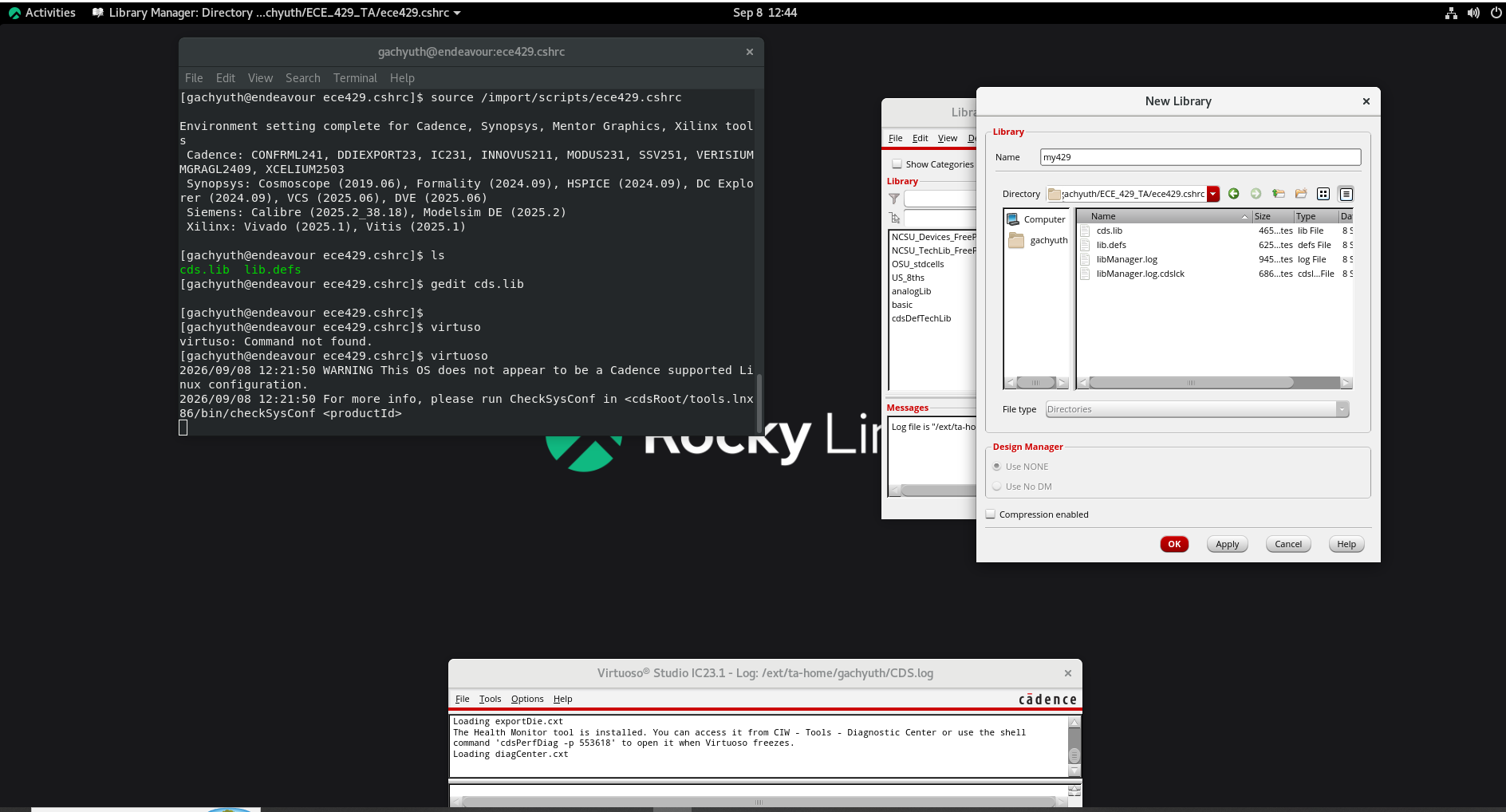
my429 library.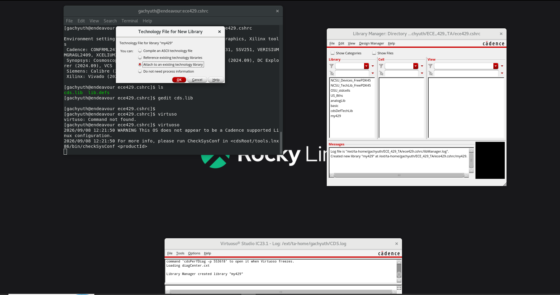
my429 once. Reuse the same library in later sessions.2.3 Create the inverter schematic
In Library Manager, select my429 and choose File → New → Cell View. Create a cell named lab02 with view schematic.
Add PMOS and NMOS devices
- Press i to open Add Instance. Select library
NCSU_Devices_FreePDK45, cellPMOS_VTL, viewsymbol, and place the PMOS. - Select the PMOS and press q. Change Width from 90 nm to 180 nm, then click Apply and OK.
- Press i again and place an
NMOS_VTLbelow the PMOS. Keep the NMOS width at 90 nm.
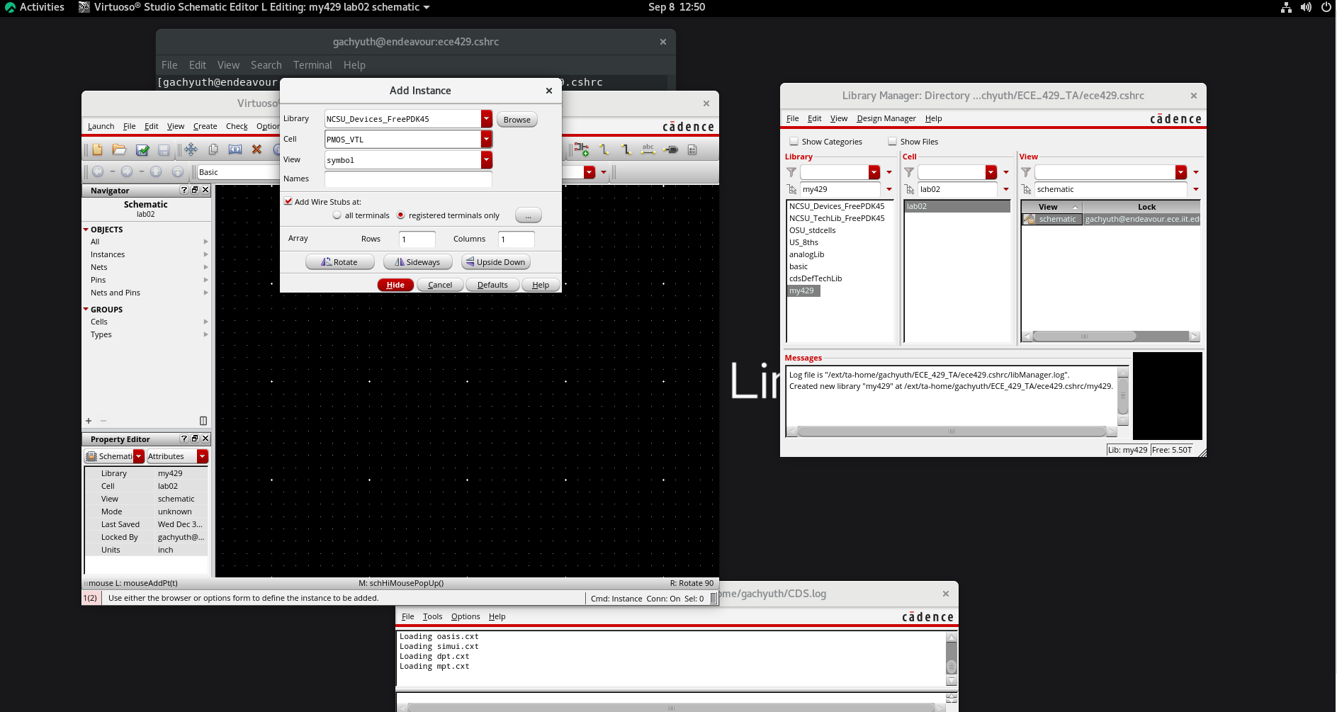
PMOS_VTL from NCSU_Devices_FreePDK45.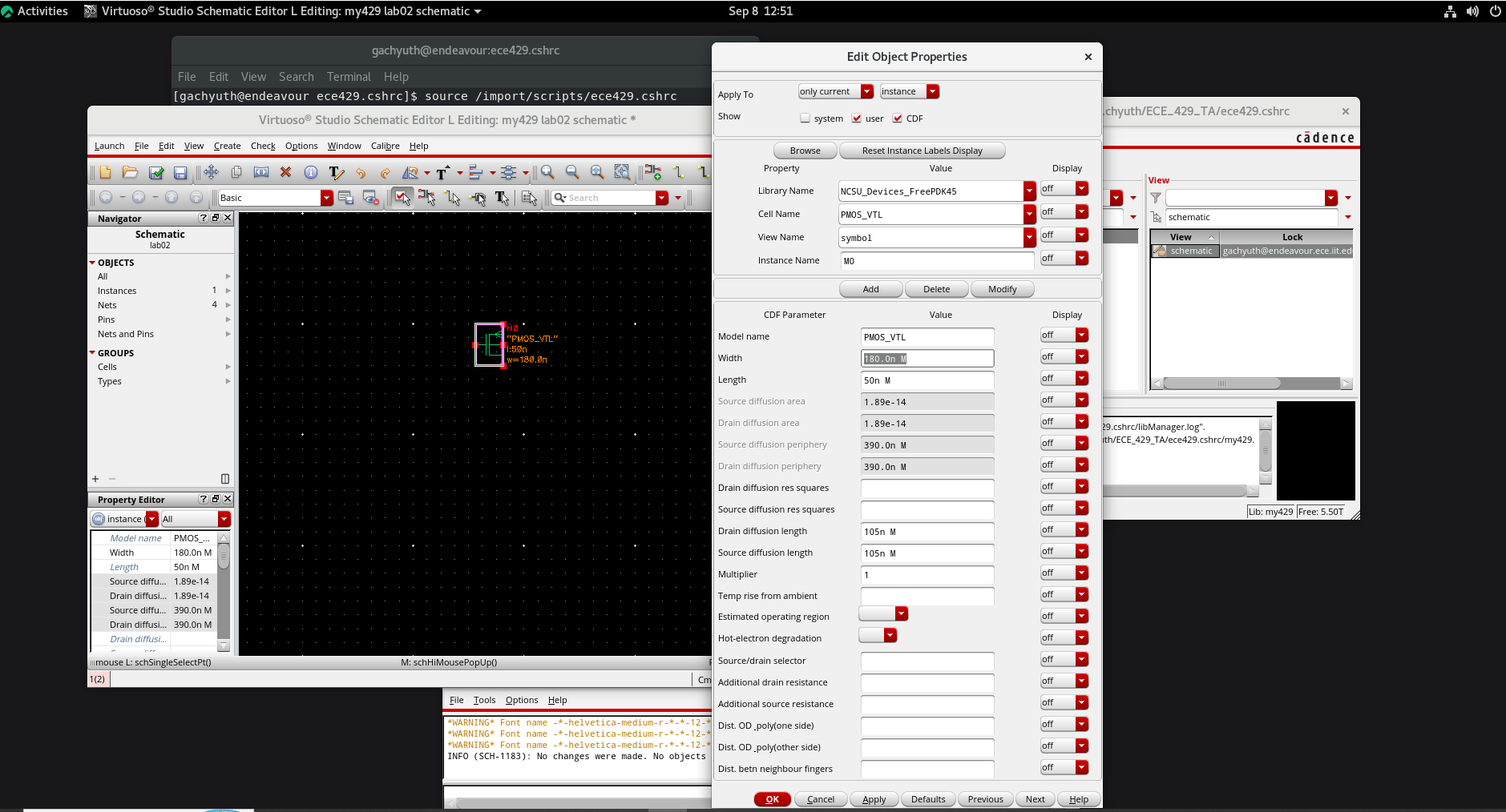
PMOS_VTL and NMOS_VTL for this lab. Do not substitute VTH or other threshold-voltage variants, because later lab steps and expected results assume the VTL devices.Add input and output pins
- Choose Create → Pin. Name the input pin
inand leave Direction = input. Place it to the left of the transistors. - Choose Create → Pin again. Name the output pin
out, set Direction = output, and place it to the right.
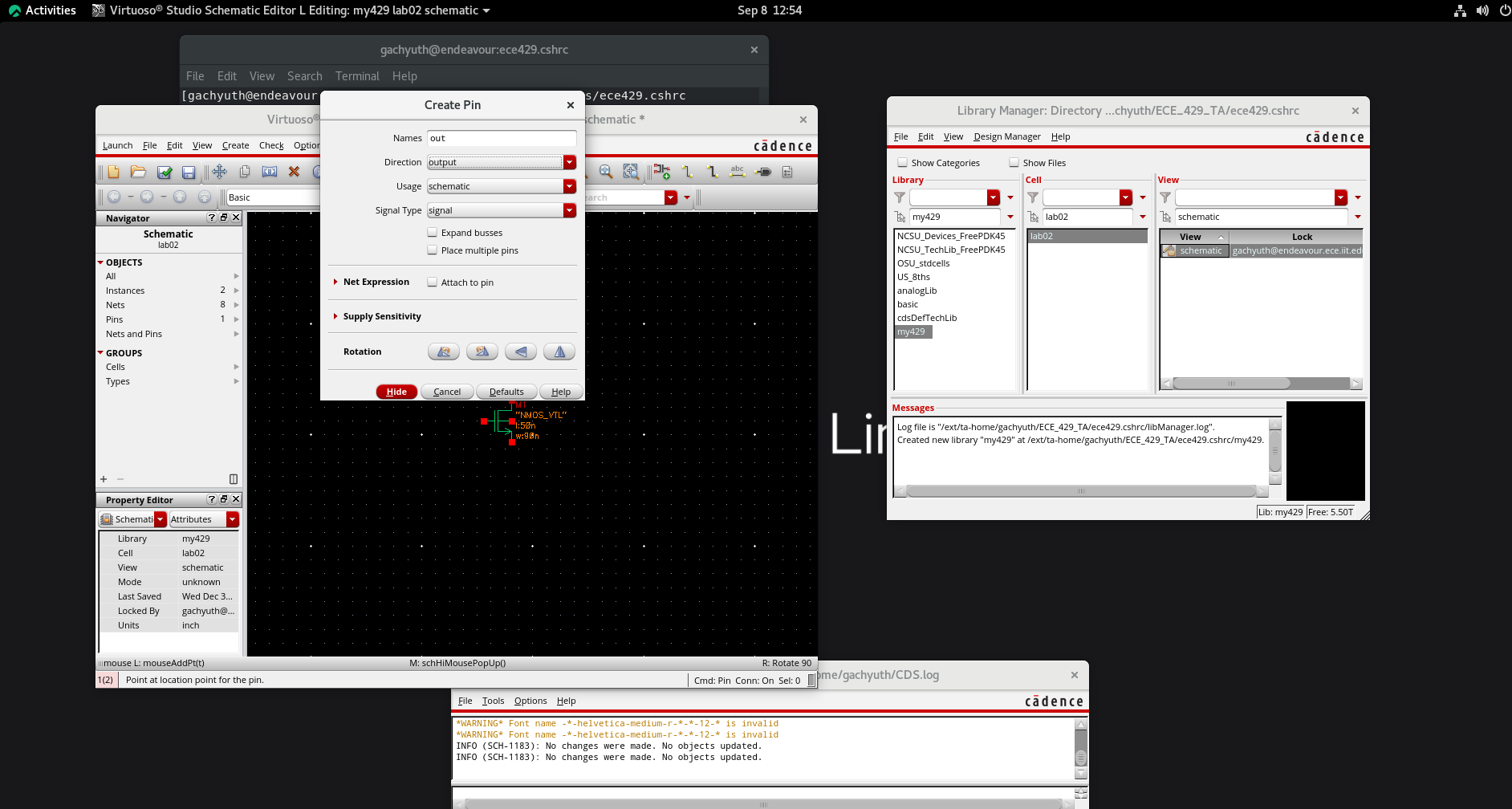
out pin with direction set to output.Add power symbols and wire the inverter
- Press i, switch the library to
analogLib, addvddabove the PMOS, and addgndbelow the NMOS. - Press w to wire the circuit. Connect both gates to
in, join the drains toout, connect the PMOS source/body tovdd, and connect the NMOS source/body tognd. - Press Esc when wiring is complete.
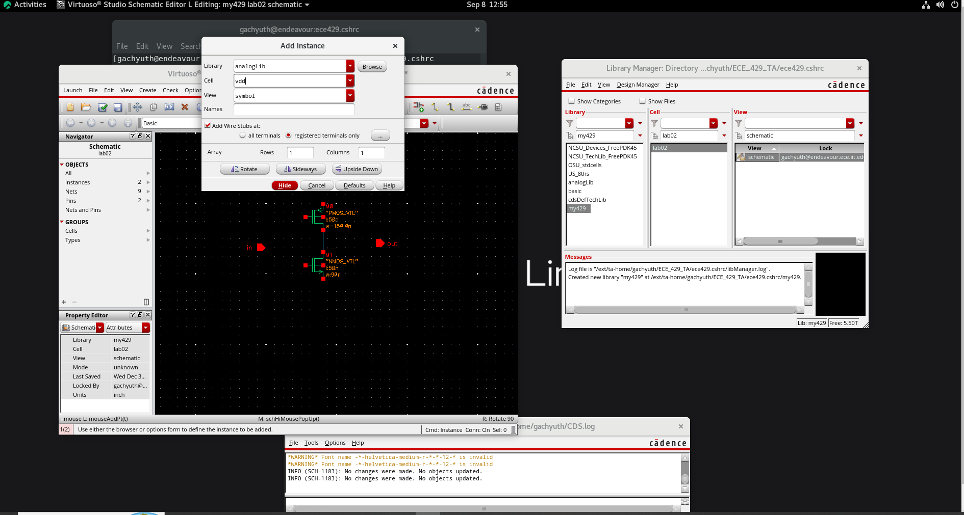
vdd from analogLib.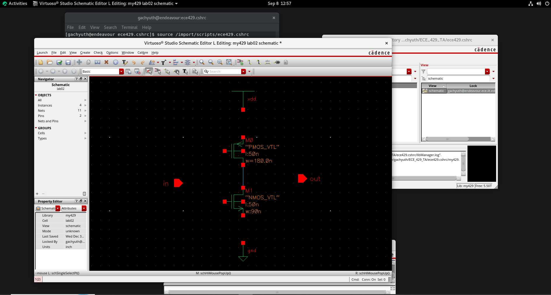
vdd above the PMOS and gnd below the NMOS.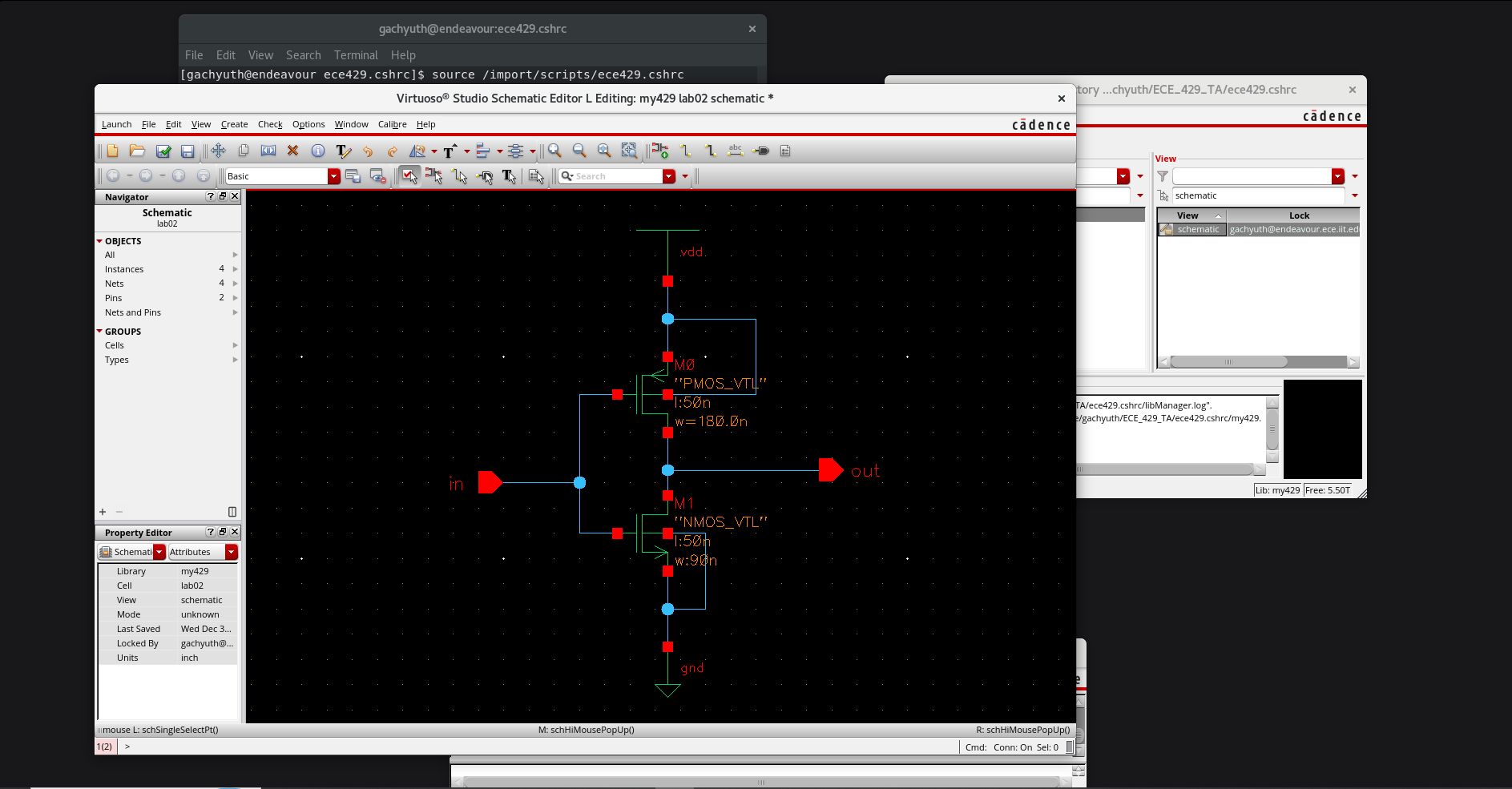
Run Check and Save. Continue only when there are no schematic errors.
2.4 Create the inverter symbol
- With the checked schematic open, choose Create → Cellview → From Cellview.
- Verify the first dialog and click OK.
- In Symbol Generation Options, verify that
inis under Left Pins andoutis under Right Pins. Keep the other defaults and click OK. - In the Symbol Editor, run Check and Save.
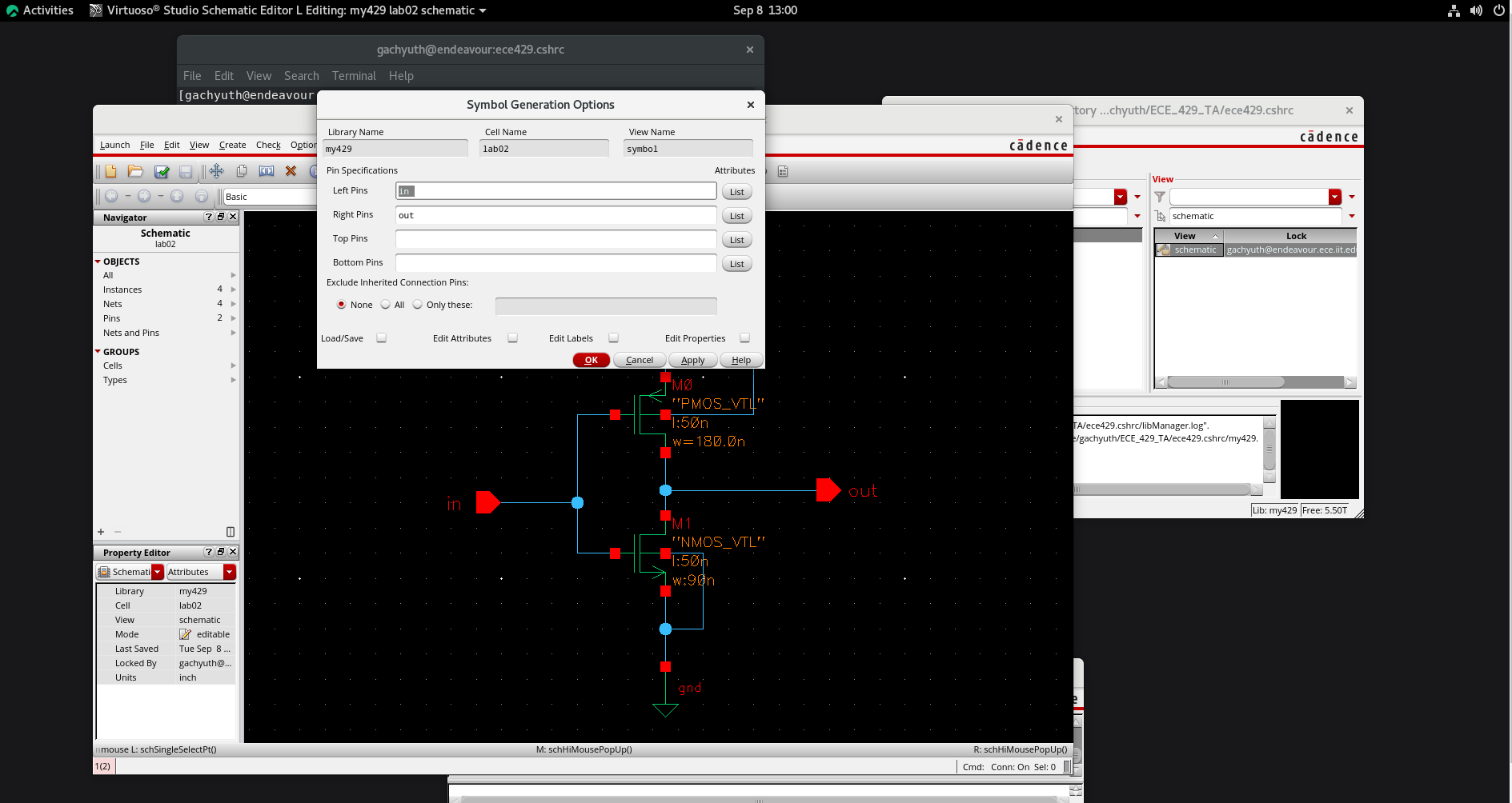
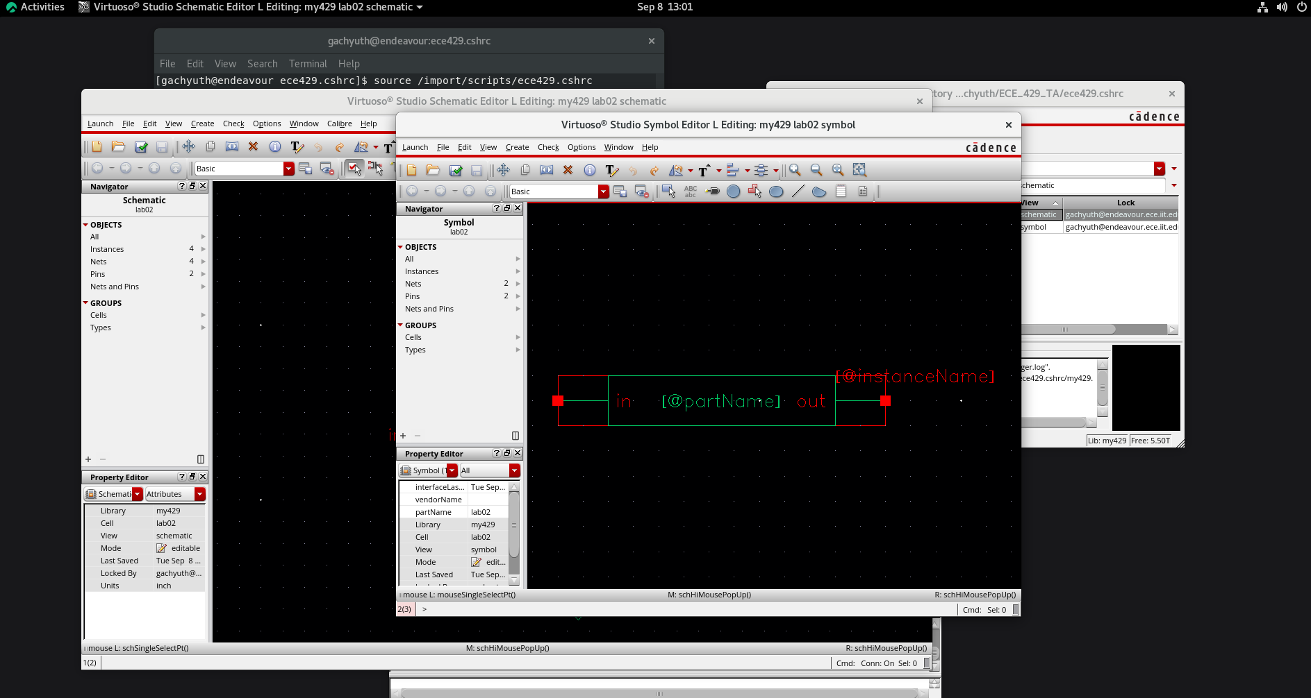
lab02 symbol.The my429 library should now contain both schematic and symbol views for lab02.
3. Inverter Simulation Using HSPICE
3.1 Create the testing circuit
Close the inverter schematic and symbol editors. In Library Manager, choose File → New → Cell View and create lab02_testing in library my429 with view schematic.
- Press i. Select library
my429, celllab02, viewsymbol, and place the inverter. - From
analogLib, addvdd,gnd, onevdc, onevpulse, and onecap. - Press w and wire the circuit as shown. Press Esc to exit wiring.
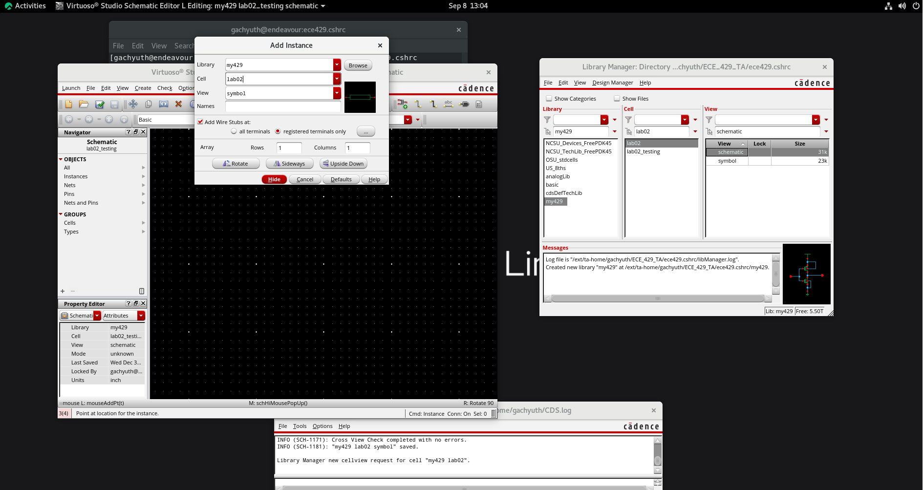
lab02 inverter symbol in lab02_testing.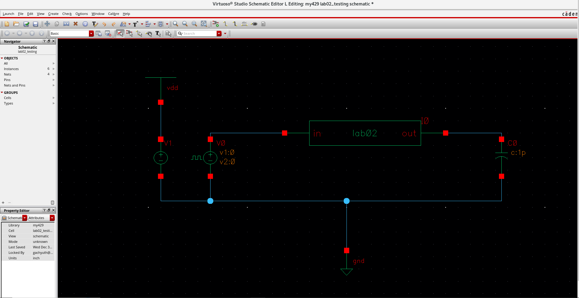
Set source and load values
Select each component and press q (or use Edit → Properties → Objects).
| Component | Required setting |
|---|---|
vdc | DC voltage = 1.1 V |
vpulse | V1 = 0 V, V2 = 1.1 V, Period = 100 ps, Delay = 0 s, Rise = 10 ps, Fall = 10 ps, Pulse width = 40 ps |
cap | Capacitance = 1 fF (change from the default 1 pF) |
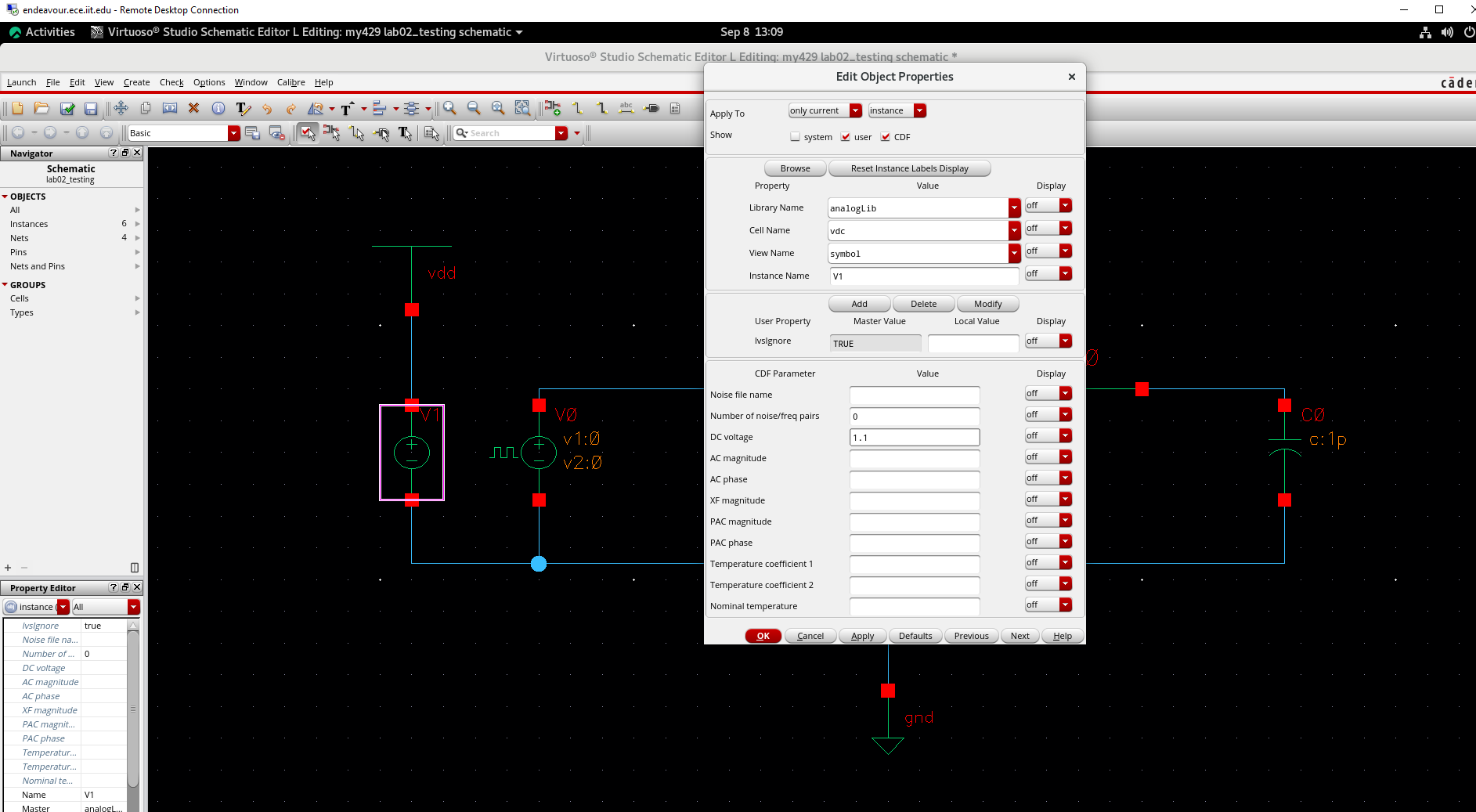
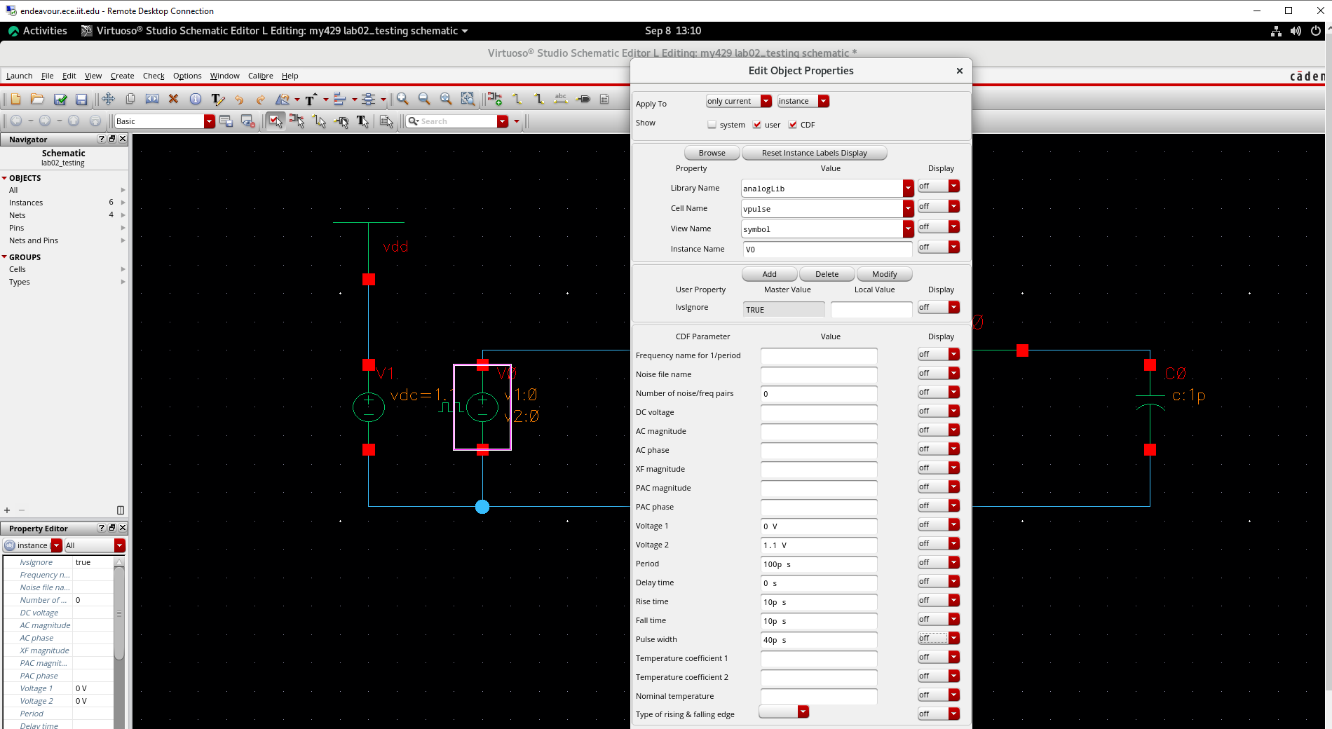
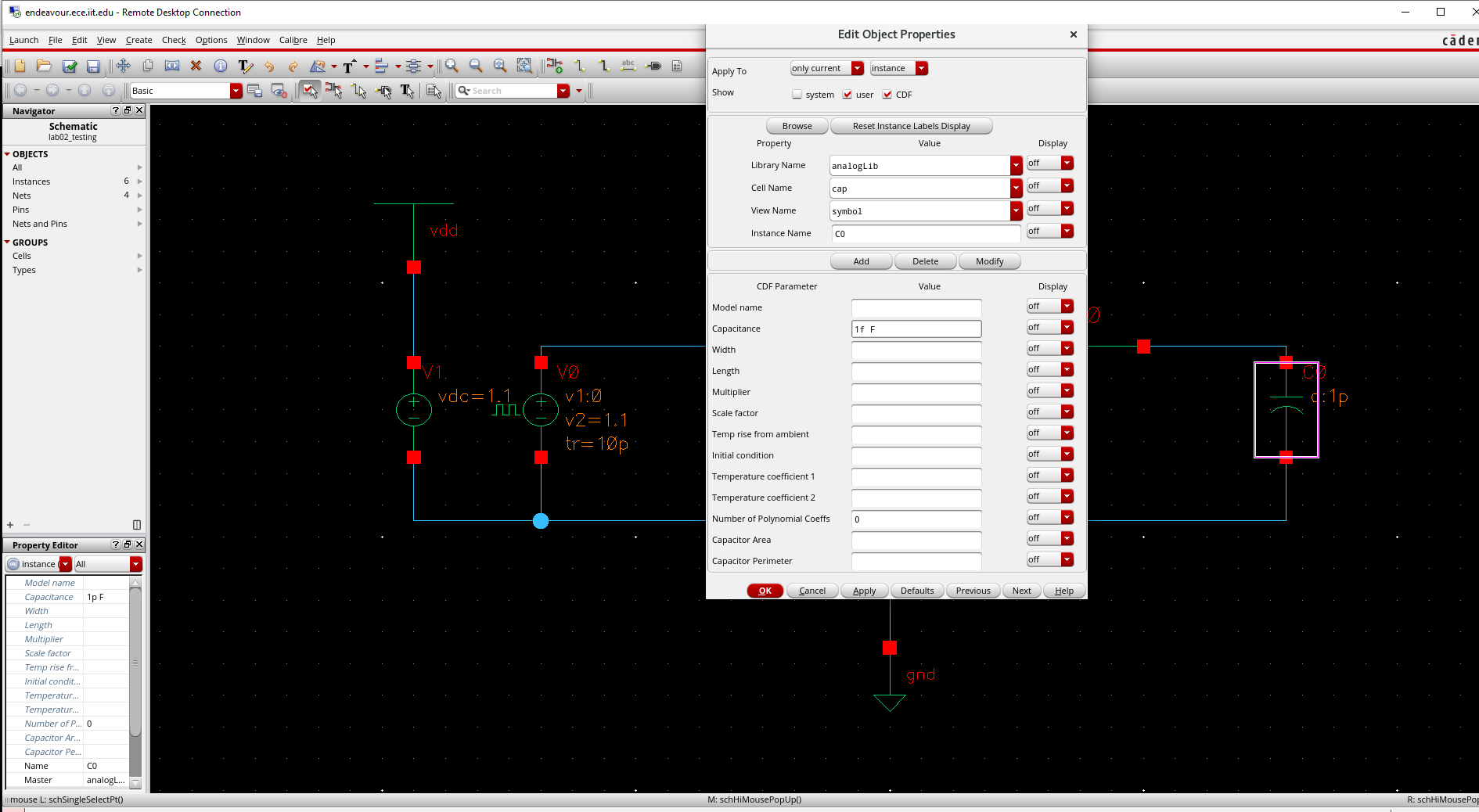
Name the input and output nets
Choose Create → Wire Name. Label the inverter input wire input and the inverter output wire output. Then run Check and Save.
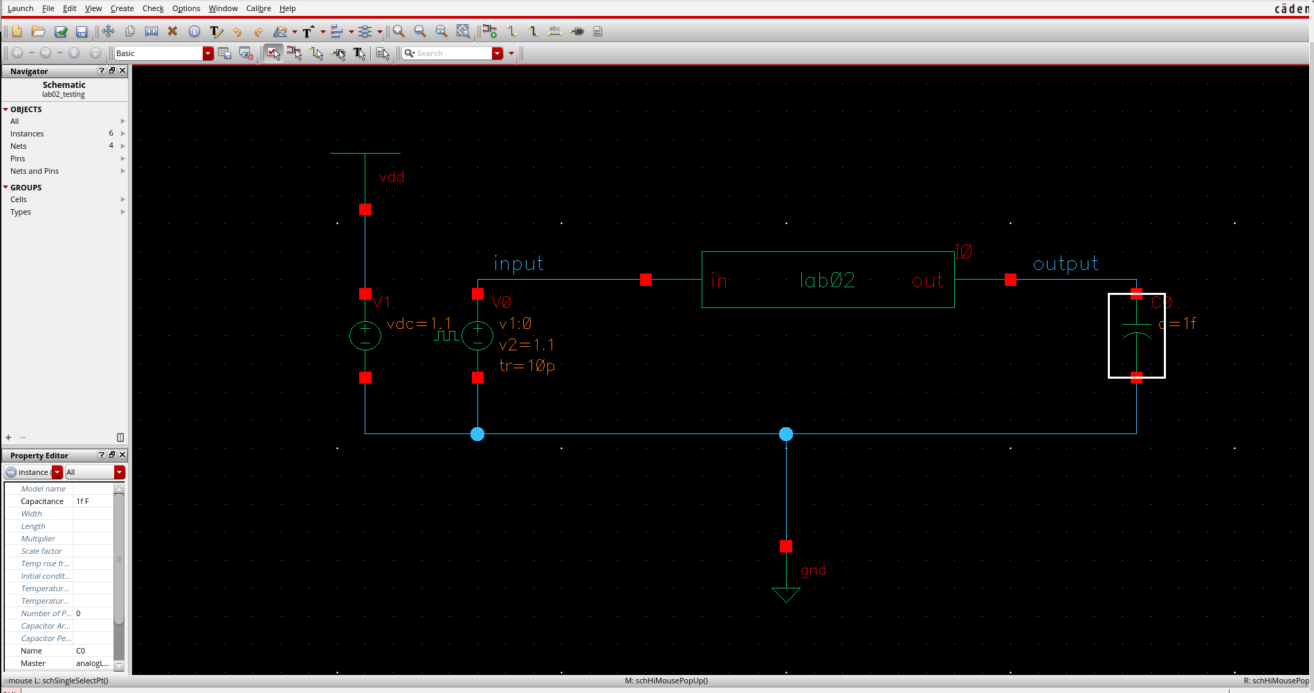
input and output net names.3.2 Configure ADE Explorer and export the HSPICE netlist
- With
lab02_testingopen, choose Launch → ADE Explorer. Select Create New View and click OK. - Choose Setup → Simulator/Directory/Host, select
hspiceD, and click OK. - Choose Setup → Model Libraries and add:
/apps/FreePDK45/ncsu_basekit/models/hspice/hspice_nom.include
Click Apply, then OK. - Choose Analyses → Choose. Select
tranand set Start =0, Stop =200p, Step =1p. Ensure Enabled is checked. - Choose Simulation → Netlist → Create.
- In the generated netlist window, choose File → Save As and save the file as
lab02.spin~/ece429.
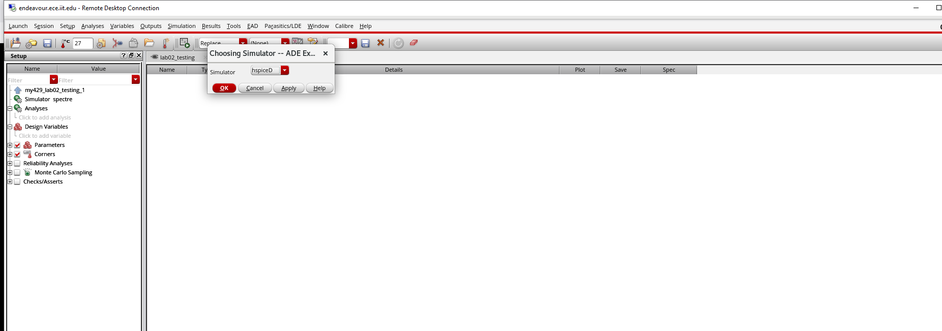
hspiceD in ADE Explorer.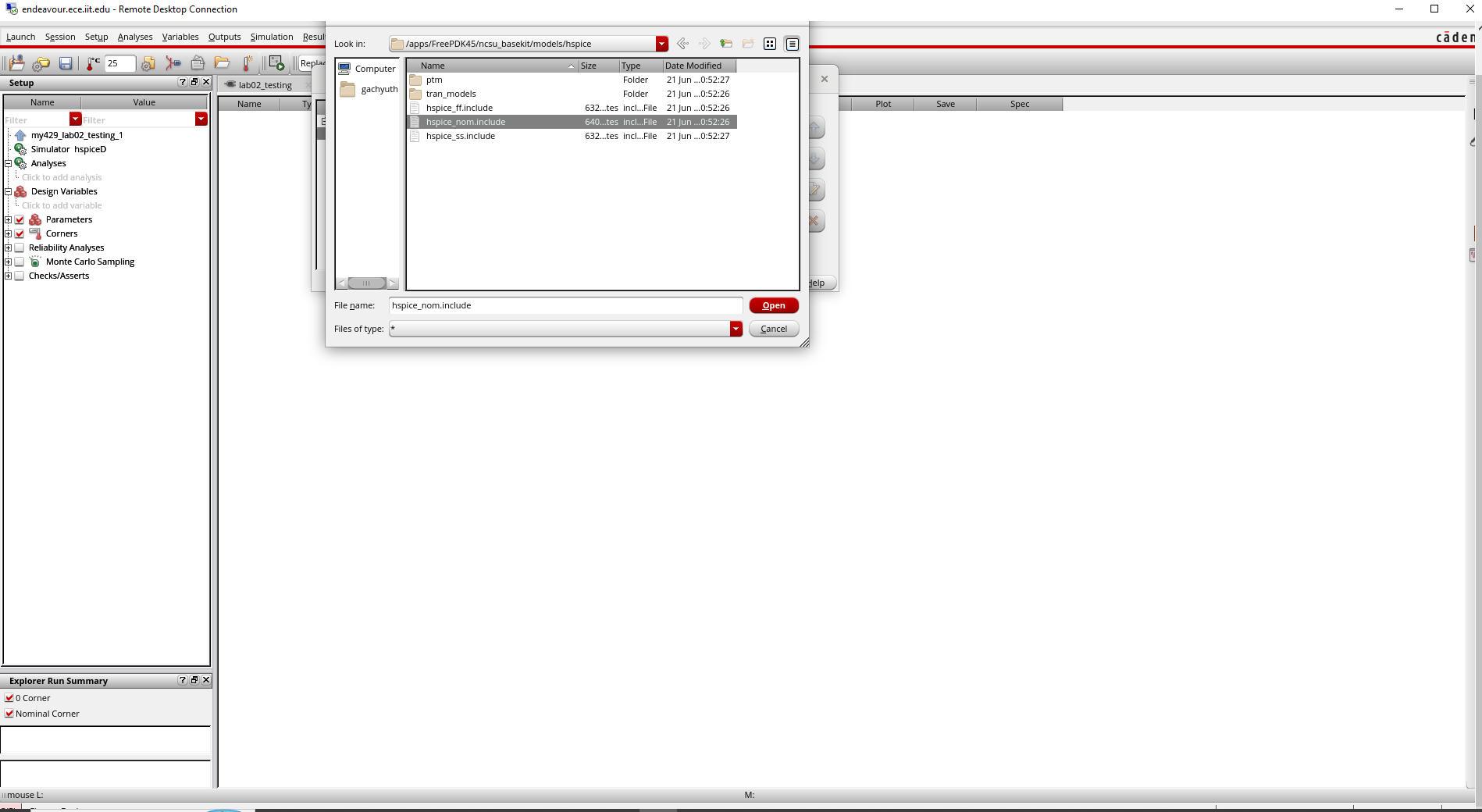
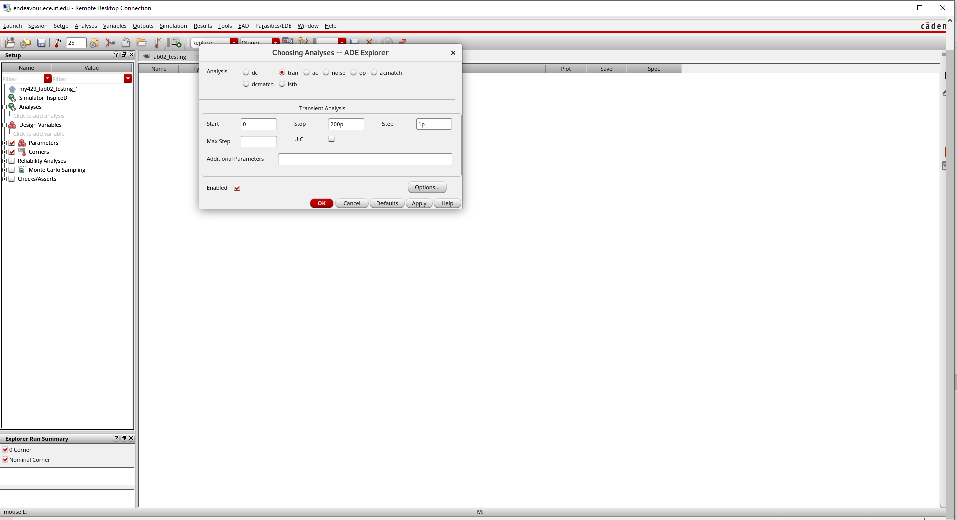
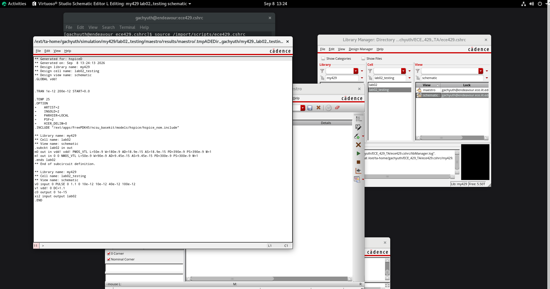
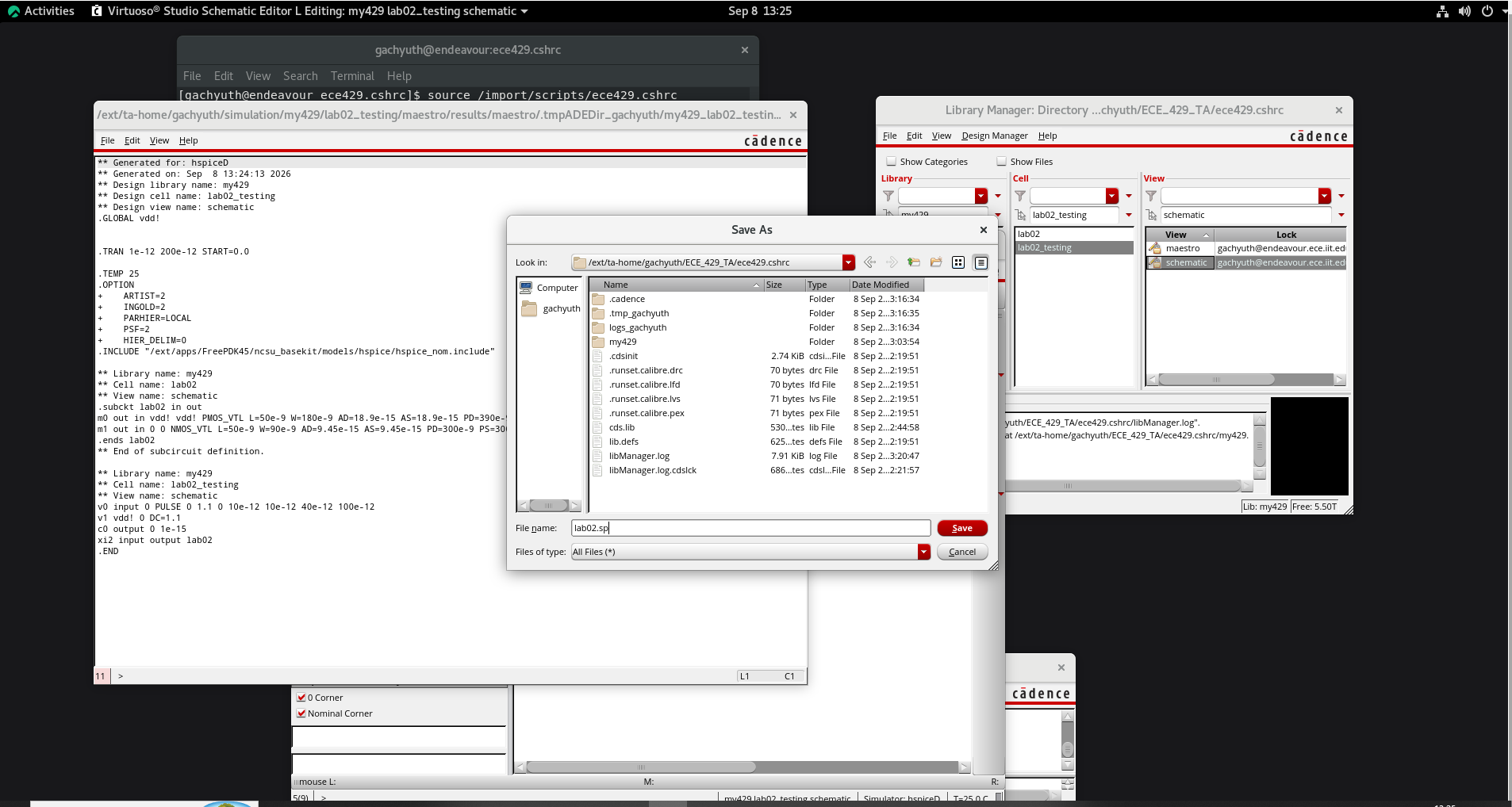
lab02.sp.3.3 Run HSPICE
In ~/ece429, verify that the netlist exists:
ls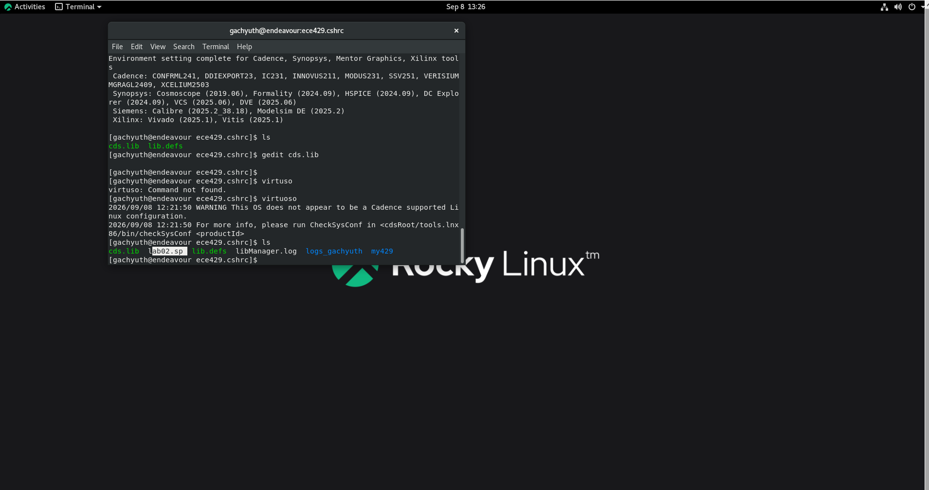
lab02.sp is present.Open the netlist in your preferred text editor. For example:
gedit lab02.spIn the .OPTION section, add + POST immediately after + PSF=2:
.OPTION
+    ...
+    PSF=2
+    POST
+    ...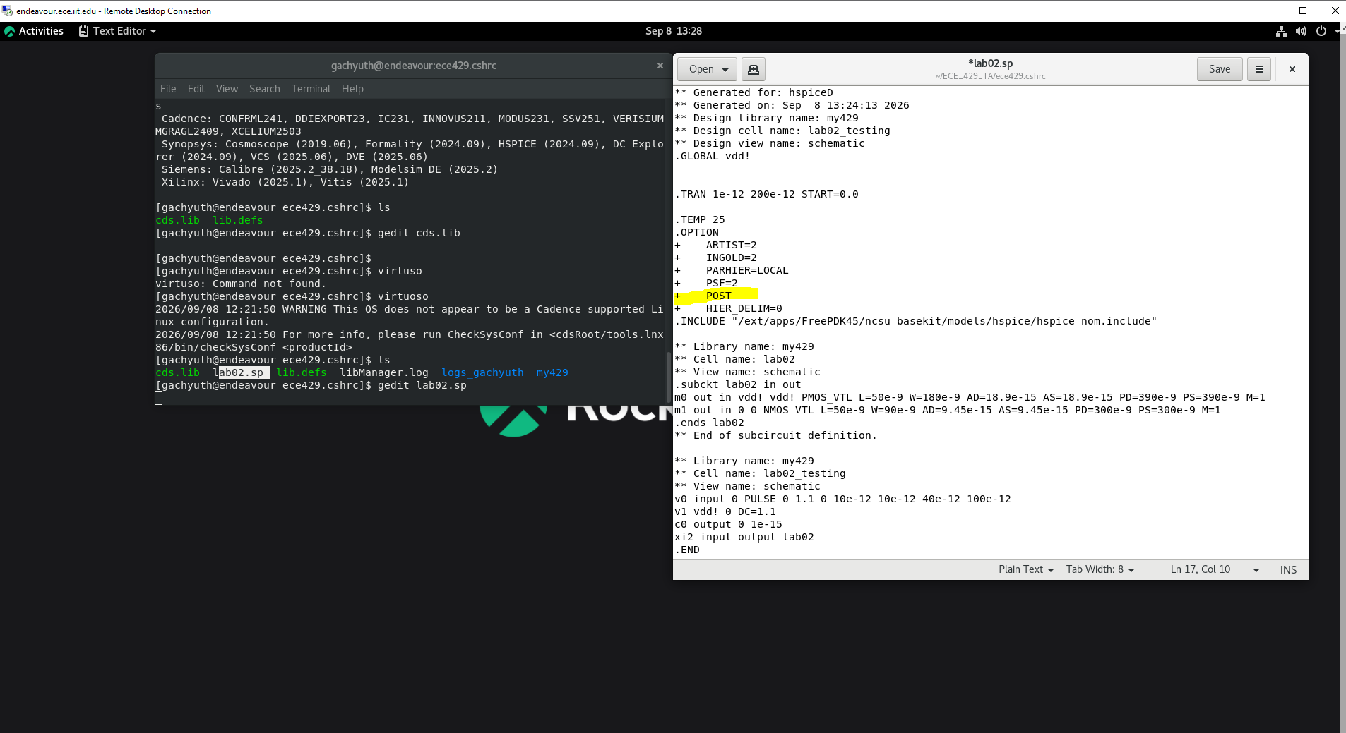
+ POST after + PSF=2, then save and close the editor.Run HSPICE:
hspice lab02.sp | tee lab02.hspice.outputThis displays the simulation log in the terminal and saves a copy to lab02.hspice.output.
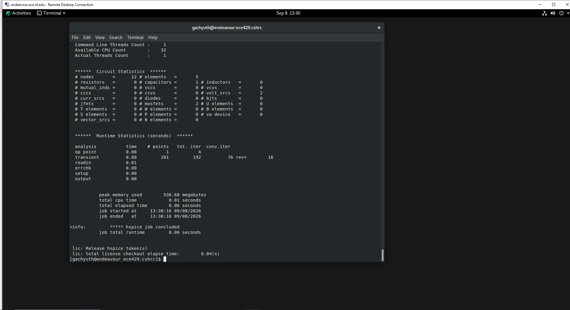
hspice job concluded. If HSPICE reports job aborted, inspect lab02.sp and the earlier setup steps. If the error remains, contact the TA.4. View Waveforms and Measure Propagation Delay
4.1 Open the waveform in Synopsys WaveView
Launch WaveView from the terminal:
wv- Choose Open Waveform, browse to
~/ece429, selectlab02.tr0, and click OK. - Double-click
D0:lab02.tr0in the waveform browser, then opentoplevel. - From the signal list, select
v(input)andv(output)and drag them into the waveform display. You may use Ctrl to select multiple signals.
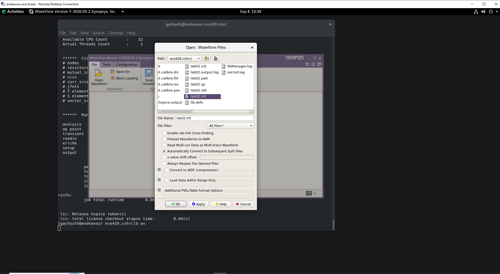
lab02.tr0.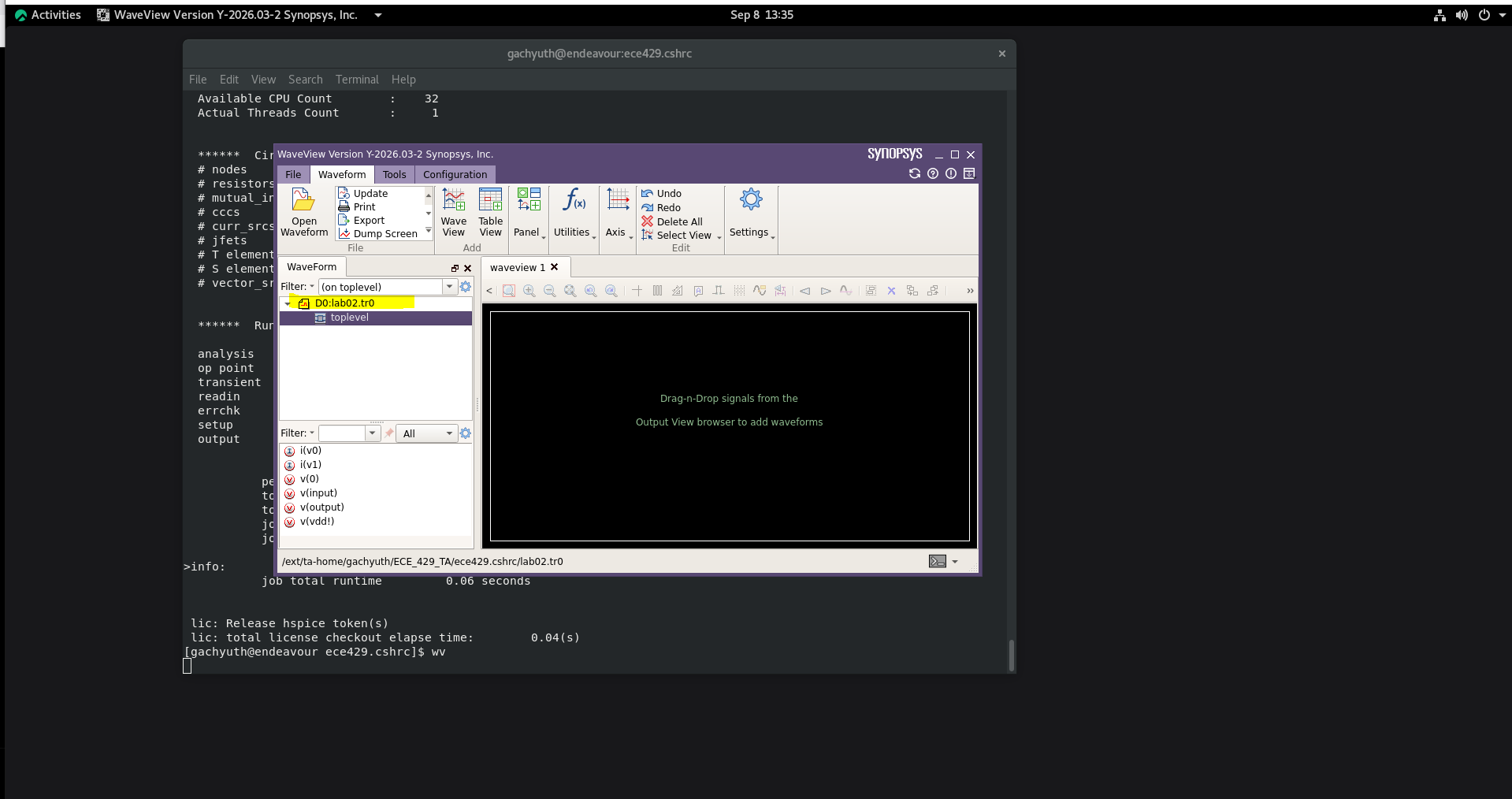
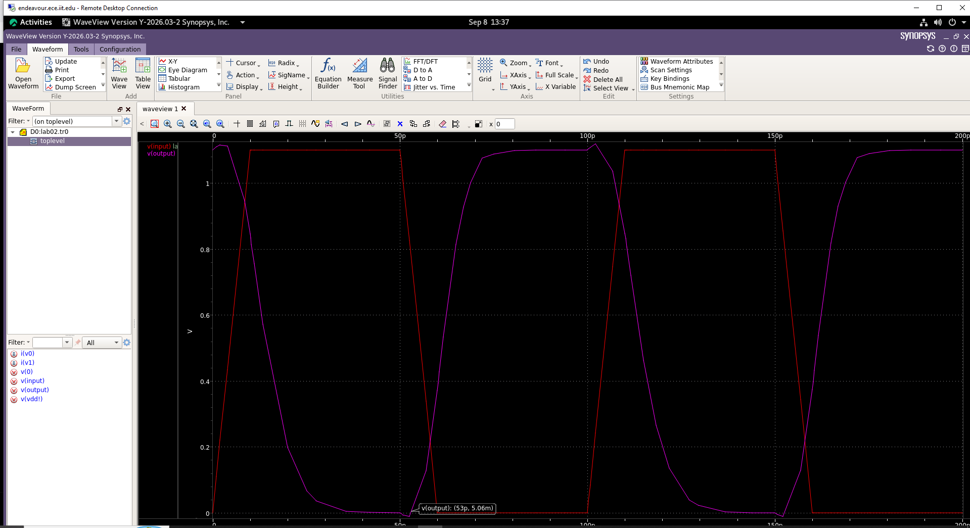
4.2 Measure propagation delay
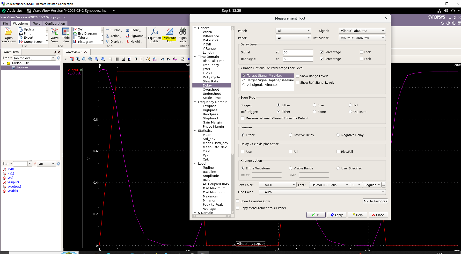
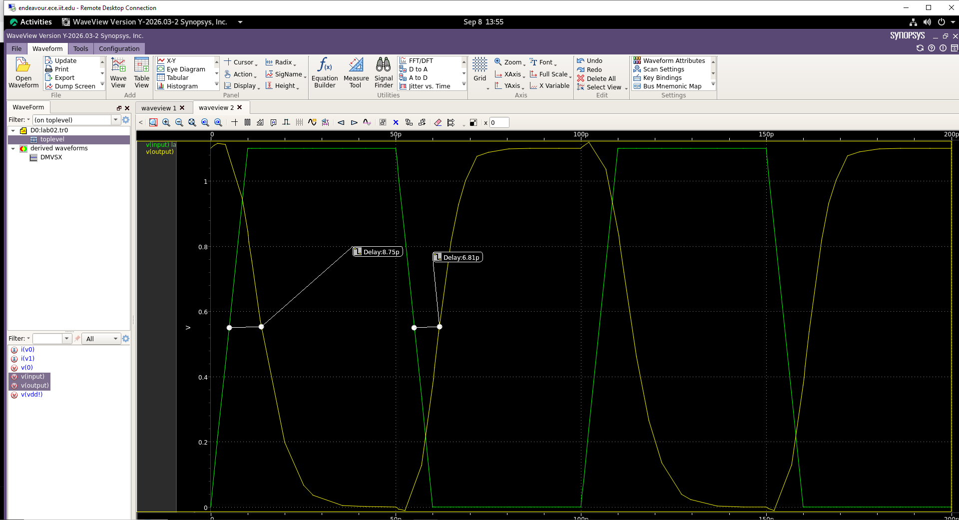
Open Measurement Tool and choose Delay under Time Domain. Use v(output) as Signal and v(input) as Ref. Signal. Set both measurement levels to 50%. For a 0–1.1 V logic swing, the 50% crossing is 0.55 V. If WaveView requests explicit top/baseline levels, use 1.1 V and 0 V.
| Delay | Output transition | Trigger | Ref. Trigger | Premise |
|---|---|---|---|---|
| tPHL | High → Low | Fall | Rise | Positive Delay |
| tPLH | Low → High | Rise | Fall | Positive Delay |
Click Apply for each configuration.
Average propagation delay
For the example waveform:
| Parameter | Example value |
|---|---|
| tPHL | 8.75 ps |
| tPLH | 6.81 ps |
| tpd | 7.78 ps |
Show delay results across the waveform
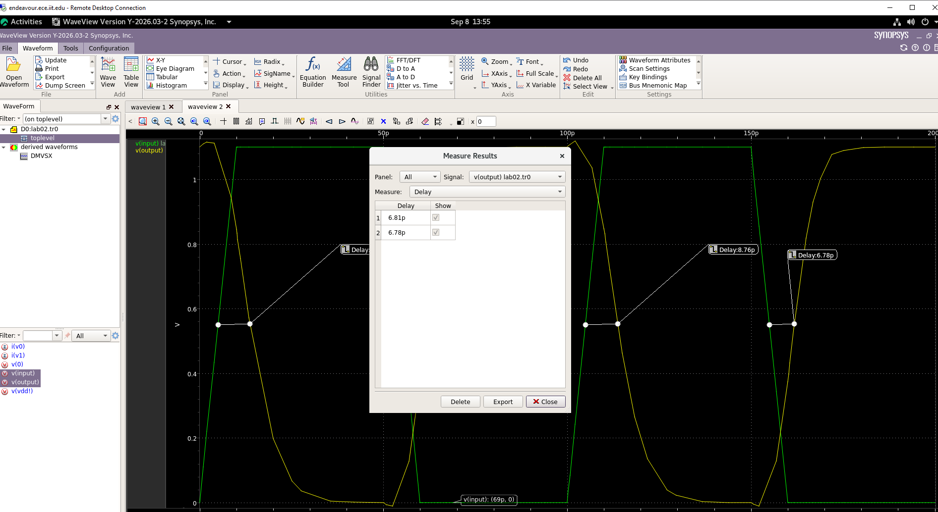
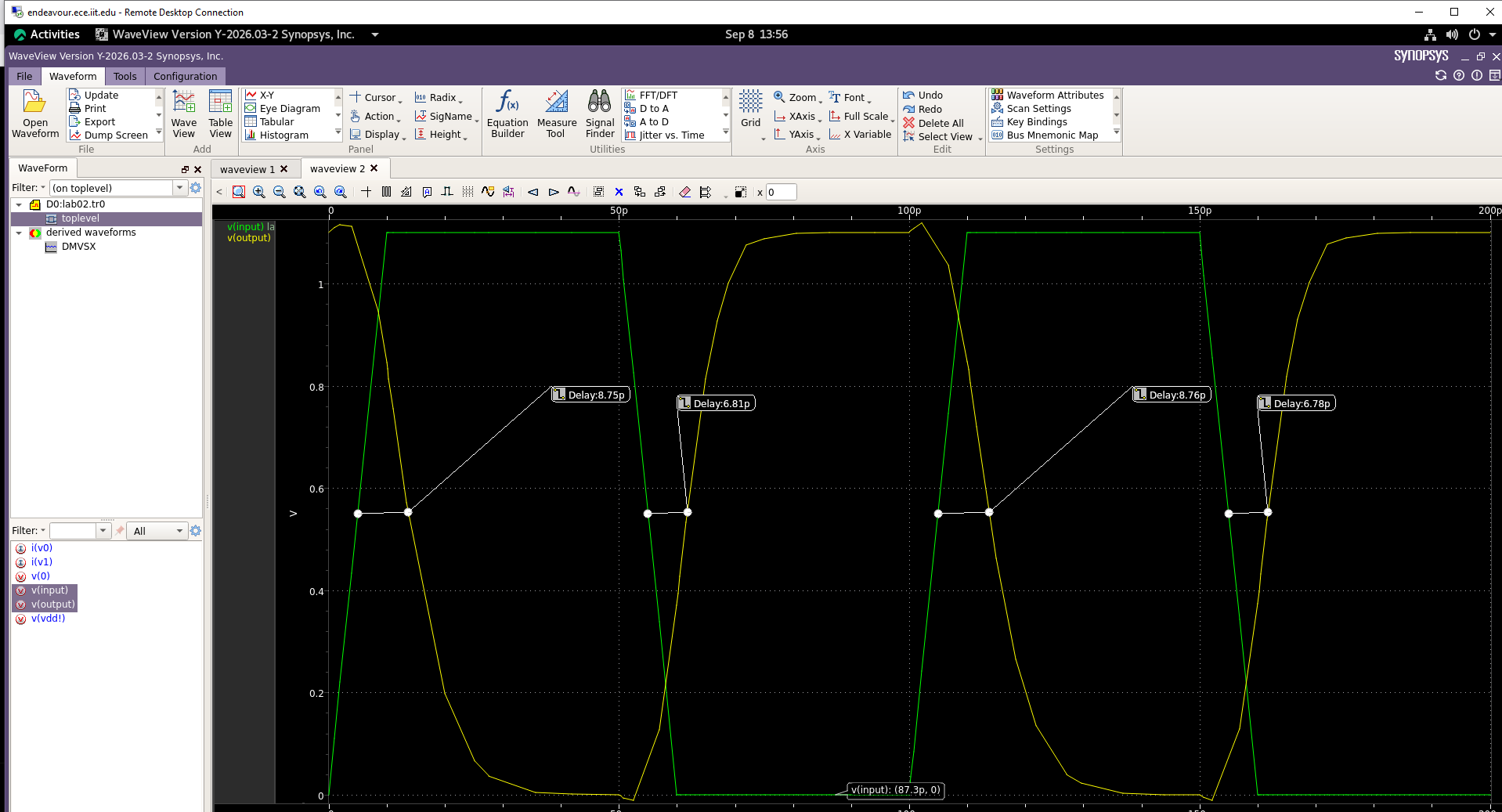
Right-click a displayed delay annotation and choose Measure Results. In the Measure Results window, enable the Show check box for the delay results you want displayed.
5. Useful Virtuoso Schematic Hotkeys
| Action | Key / method |
|---|---|
| Add instance | i |
| Edit object properties | Select object, then q |
| Draw wire | w |
| Name wire | l or Create → Wire Name |
| Move object | m |
| Exit active command | Esc |
Virtuoso also displays mouse-button actions and command hints in the status area at the bottom of the editor.