Standard Cell Based Design
using Cadence PKS, Cadence Silicon Ensemble, Synopsys PrimeTime and Magic 6.5
Johannes Grad and James E. Stine
Illinois Institute of Technology
Department of Electrical and Computer Engineering
3301 S Dearborn
Chicago, IL 60616
Table Of Contents
3) Post-Synthesis
Verification
7) Layout-Versus-Schematic
(LVS) Verification
1) RTL Simulation
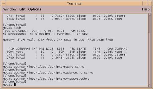
Before you do anything, be sure to run the following three commands whenever you open a new terminal:
source /import/app1/scripts/magic.cshrc
source /import/app1/scripts/cadence.ic.cshrc
source /import/app1/scripts/synopsys.cshrc
The source commands will give you access to Magic, the Cadence tools and the Synopsys tools. See the figure below for a typical screen:
Typically you enter code in Verilog on the Register-Transfer level (RTL), that is you model your design using clocked registers, datapath elements and control elements. You will use Cadence Verilog-XL to simulate your design. You will also need to create a Verilog testbench for your circuit.
In this tutorial there are 2 files. You can find their contents in the Appendix.
- accu.v Verilog RTL code for an 8-bit accumulator
- accu_test.v Verilog testbench for accu.v
In order to simulate Verilog code, use this command:
verilog accu.v accu_test.v
See the following Figure for the output:
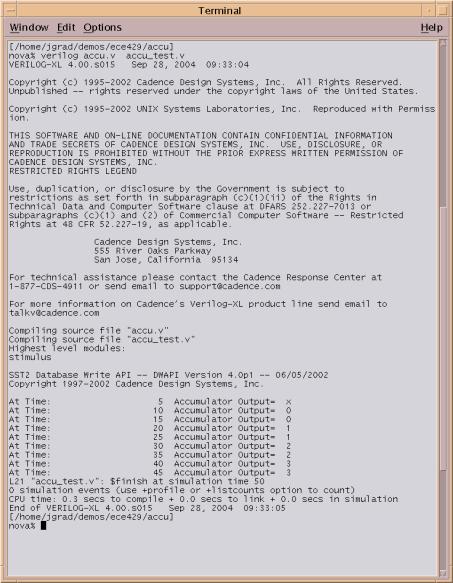
This testbench provides results directly on the screen and also in a waveform database. From the screen we can see that the design behaves as expected. That is, every 10ns we add "1"” to the accumulator. This is expected since "in" the testbench a clock of 10ns is specified and the input "in" is connected to a constant "1"”.
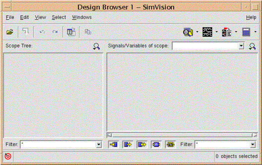
We use the program Cadence Simvision to look at the waveform database that was created by Verilog-XL. Type the following command:
simvision&
The "&" symbol tells the operating system to return to the console so you can continue to type commands while Simvision runs in the background. This is just convenience and nothing essential. Simvision will look like this:
Now we need to open the Waveform database. Click on the "Open"” symbol.
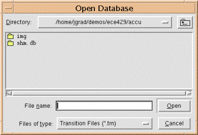
Then double-click on "shm.db"”, which is the folder where the file is located.
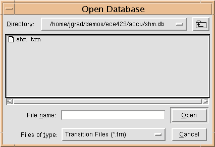
Inside the folder is only one file, shm.trn. Double-click on the file to open it. To see the contents of the waveform database, click on "stimulus"”:
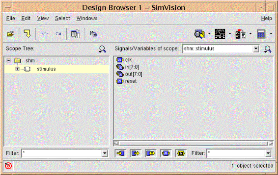
Now we want to plot our waveforms. We need to select which signals we are interested in. In this case lets look at all waveforms. Select all 4 waveforms on the right:
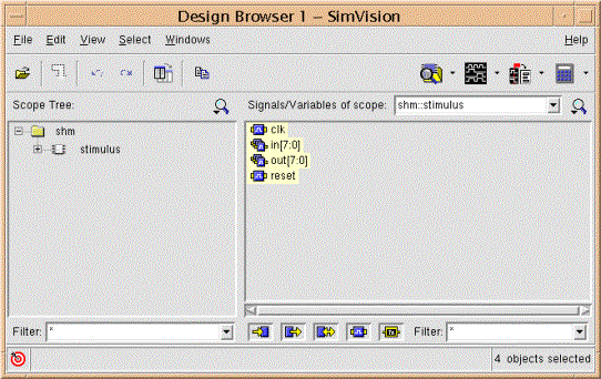
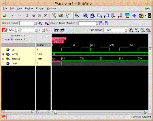
Then hit the third picture-button from the left, the one with the square waves. We see that the circuit works fine. At every rising clock edge the output changes. Now exit Simvision.
2) Logic Synthesis
Once you have verified that your Verilog RTL code is working correctly you can synthesize it into standard cells. The result will be a gate-level netlist that only contains interconnected standard cells.
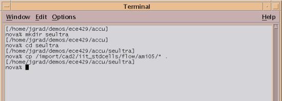
There are template files for all the following steps already prepared for you. We will now copy those templates into our project. To keep things organized we will run synthesis in a separate folder. That way it will be separate from the original RTL code. Use the mkdir command to create a folder. Then copy the templates, as shown below:
mkdir seultra
cd seultra
cp /import/cadence1/osu_stdcells/flow/ami05/* .
Now we have created a folder “seultra” and filled it with the template files for the AMI 0.5um technology.
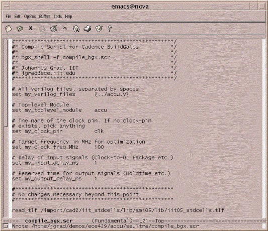
We will use the tool Cadence PKS for logic synthesis. Another popular tool is Synopsys Design Compiler. The template file for PKS is called “compile_bgx.scr”. Note that “bgx” stands for BuildGates Extreme, which is the software package that contains PKS.
Now we will open “compile_bgx.scr” in a text editor and modify it according to our accumulator design. This file is a command file for PKS and will be executed line by line. To make it easier to modify, all key values are defined in the beginning of the file. So the only modifications will be done in the header of the file. Specifically, we need to change the following for values:
|
my_verilog_files |
../accu.v |
The RTL input file that we want to synthesize. |
|
my_toplevel_module |
accu |
The name of the top-level module in the RTL code. |
|
my_clock_pin |
clk |
The name of the clock pin in the RTL code |
|
my_clock_freq_MHz |
100 |
Tells PKS to optimize the circuit so that it is capable to operate at least at 100 MHz. |
Later, once you have more experience, you can take a look at “compile_bgx.scr” and look at the different commands that are used to read in RTL code, optimize it and output gate-level code. But for now it is enough to just plug in our desired values in the header of the file. You can use any text editor. Most professionals use “emacs” but some people prefer the simpler “pico”.
Now that we have a command file for PKS we can go ahead and run it:
pks_shell -f compile_bgx.scr
PKS will run for a short time and create substantial amounts of output. When it is finished it will return to the command line. If there is an error PKS will specify the exact source of the error and the line number in the command script that was responsible for the error. Typically there will be no errors. The screen after running PKS will look like this:
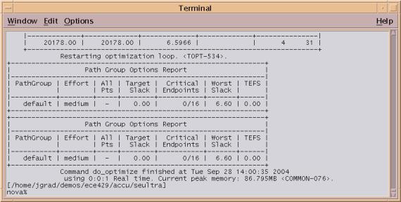
A quick look at the last lines of output tells us that “the Worst Slack is 6.6 nano seconds”. The most important number in digital logic design is the “Slack”, or the safety margin we have with respect to the clock frequency. More about this in the following:
To get more detail regarding slack and timing we look in the file “timing.rep” that was created by PKS. It contains very detailed timing information about our circuit. To see the file use “cat”, which displays text files:
cat timing.rep
It will look like this:
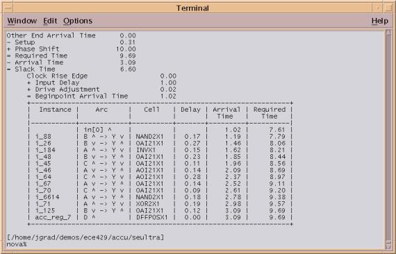
The first thing we notice is the “critical path” of our circuit. This is the path of logic that has the longest delay and, therefore, is the upper limit on the clock frequency. The clock frequency cannot be faster than the inverse of the delay of the critical path. When we look closer we see that the critical path starts at the input pin “in[0]” and ends at the “D” pin of a D-Flip-Flop. A critical path can be anywhere in the circuit: from an input to a register, from a register to the output or between two registers. If the circuit is combinational, that is it has no registers, then the critical path will always be between an input and an output.
The last line of “timing.rep” tells us that the delay of the critical path is 3.09ns. And in order to be able to operate at 100MHz the required time of the critical path has to be below 9.69ns. Hence the “Slack”, which is the difference between the two:
9.69ns-3.09nsn = 6.60ns.
In this case we are well within the limit. The critical path could be up to 6.6ns longer and we would still meet our goal of 100MHz. This means we could compute the theoretical maximum operating frequency:
![]()
This means if were to fabricate the current circuit we could operate it at a speed of up to 323MHz. But what we could also do is the following: We could go back to “compile_bgx.scr” and change the target clock frequency from 100MHz to 350MHz. That would force PKS to optimize our circuit more than previously. That is, it has to try to shorten the critical path, using Boolean arithmetic, in order to get its delay below 2.86ns, which is the inverse of 350MHz.
Note that these calculations are somewhat simplistic. Since we originally specified 100MHz, we might expect the limit on the critical path to be simply the inverse, or 10ns. In reality we see that the requirement is 9.69ns. For example, we neglected the setup time of the D-Flip-Flop. The signal must reach the input of the Flip-Flop some time before the clock edge, in order to be reliably stored. In addition, we also assumed some initial delay on the input signal, which could be the delay of the IC package, or the delay of the gate that produces the signal on “in[0]”.
If you want to know immediately how fast your circuit is, set the target frequency to an impossible high value, e.g. 3000MHz, which is 3GHz. That will force PKS to produce the fastest possible circuit. Then we can see from “timing.rep” what the fastest possible clock frequency is and plug it back into “compile_bgx.scr”. But you have to realize that PKS will try very hard to meet your impossible target, resulting in a long run time and a very big circuit with many extra gates.
As a final exercise, we can look at the output of PKS. As we said above, it is a gate-level Verilog netlist that only contains interconnected standard cells. The netlist will be called accu.vh:
emacs accu.vh
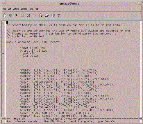
Note that the top-level module still has the name “accu” and the names of the inputs and outputs has not changed. From the outside it is exactly the same circuit as you coded on the RTL level. But on the inside all functionality is now expressed only in terms of standard cells. Since we have layouts for all standard cells, we can now easily place and route them for the final layout. But before we do that we perform another round of verification because we want to make sure our circuit behavior has been persevered during the transition from the RTL level to the gate level.
3) Post-Synthesis Verification
Since the gate-level netlist is also in Verilog format we can use the same Verilog-XL command line we used for RTL level simulation. In addition, since we are now using standard cells, we need to include an extra file “osu05_stdcells.v” that includes definitions for all standard cells. Use the following command:
verilog osu05_stdcells.v accu.vh ../accu_test.v
Note how we re-used the original testbench from the RTL level simulation. That is an excellent way to ensure that the gate-level representation matches the RTL level. Since we are now working in the “seultra” folder we used the “../” notation to signal the operating system that “accu_test.v” is located one folder above the current folder.
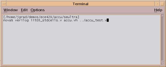
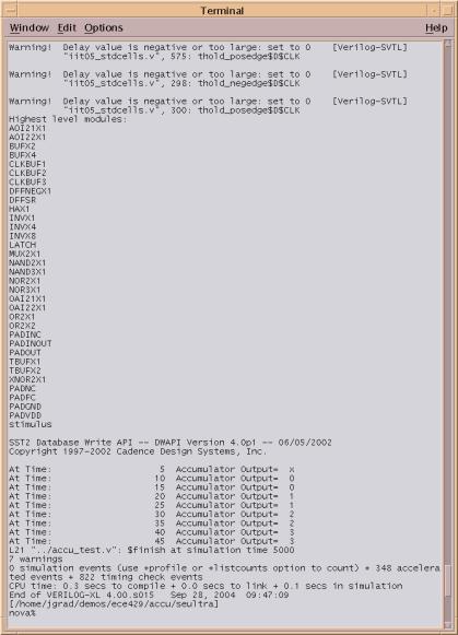
The Verilog simulation looks similar to before. Ignore the osu05_stdcells.v warnings.
4) Place And Route (P&R)
At this point we have synthesized our original Verilog design, which was implemented on the RTL level into a gate-level design. We also verified that the synthesis result is still correct by using our original testbench.
Now we can use Cadence Silicon Ensemble to place the standard cells and route them. The result will be the final mask layout that could be shipped to the AMI foundry for fabrication.
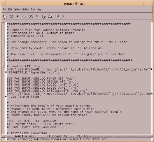
The template file for Silicon Ensemble is called “seultra.scr”. Just like before, it is a command file that is executed line by line. It includes commands to input the gate-level netlist, floorplan the chip, place the cells, route the cells and to verify the layout. In the end, the final layout is written in GDS-II format, which is the most popular format for IC layouts. It can be imported into Magic and many other layout tools.
All we need to do in “seultra.scr” is specify the input file as “accu.vh” and the top-level as accu. See below for the final file:
Now we are ready to run Silicon Ensemble. The command line is
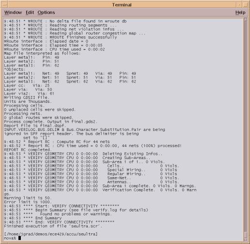
se_shell -f seultra.scr
The last steps are “Verify Geometry” and “Verify Connectivity”. This is done to ensure that the layout has no design rule violations and that there are no short or open wires. The final output is seen below. Note that there are zero geometry and connectivity violations:
5) Static Timing Analysis
At this point we can find out the new “Slack” of our design. It will be less than we had after synthesis. That is because now we have physical wires, which have non-zero delays. The timing report after synthesis assumed zero wire delay. In order to model wire delay Silicon Ensemble extracted the capacitance and resistance of all wires in the layout and saved them into a file.
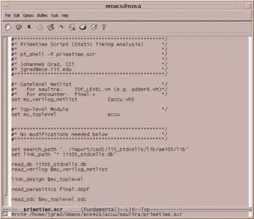
We will use the tool Synopsys Primetime to create a new timing report. This time we will import the gate-level netlist so we can compute the gate delays, as well as the parasitic information, so we can compute the wire delay. Primetime will then determine the new critical path delay.
The template file for Primetime is called “primetime.scr”. All we need to do is specify the netlist name, which is “accu.vh” and the top-level name, which is “accu”. See here for the complete file:
Now we are ready to run Primetime:
pt_shell -f primetime.scr
Assuming there are no errors, we will get a timing report called “timing.rep.pt”. Open it using
emacs timing.rep.pt
It will look like this:
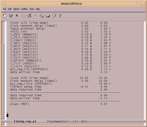
Note that the slack is now only 6.57ns, which is less than the 6.6ns we had before. But we can also see that the difference is very small. We are working with a very small design, so all the wires are very short and have little delay. If we had a large circuit we would see a substantial delay contribution by the wires.
Note the word “MET” in the last line. Primetime is telling us that we met our goal of 100MHz. Had we not met the goal, i.e. if our slack was negative, we would get the word “VIOLATED”, which means that we violated our timing constraint of 100MHz.
Finally, note that our critical path is still the same as before, i.e. between “in[0]” and the pin “D” of acc_reg_7. If the wires in our design were longer and had less delay the critical path would likely be different now. We see that as we progress to lower and lower levels of abstraction we get more detailed information about the behavior of our circuit. But it would also take longer to fix the circuit if we were to find out that we would no longer meet our timing constraint. We would have to re-do synthesis and place&route and possibly even modify the RTL code. For large designs, it might take days or weeks to perform one such iteration. That is why it is necessary to have sophisticated tools that provide good timing estimates early in the design flow.
6) Schematic Simulation
Now we have created our final layout. Now we need to perform another round of verification to ensure that our layout is actually what we wanted, i.e. it has the same behavior as our original Verilog description on the RTL level.
We will use two methods of verification:
- We will simulate some clock cycles to see if the layout behaves as expected. However, since a full chip typically contains thousands or millions of transistors, this simulation will take a very long time. Hence we can not exhaustively simulate the complete chip.
- We will perform LVS comparison to a schematic. Since the schematic is derived from the gate-level netlist we can easily catch inconsistencies introduced by Silicon Ensemble, e.g. an open wire or a short
In this step we will create a Sue schematic and create a sim file from it. We will also simulate it in irsim to ensure its basic correctness.
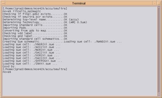
There is the command “osucells_se2magic” that will create both, a Magic layout and a Sue schematic. Run it without any parameters:
osucells_se2magic
The output will look as follows:
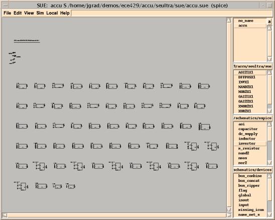
The Sue schematic will be created in a folder called “sue” and will be called “accu.sue”. Open it as follows:
cd sue
sue accu.sue
It will look similar to the following screen. Note that the schematic was derived from the gate-level netlist, so it only contains a large number of standard cells and little else.
To create a sim file, use the typical procedure:
Sim | Change Simulation Mode… | Select “Sim” mode
Sim | SIM Netlist
This will create the file “accu.sim”. Now exit Sue.
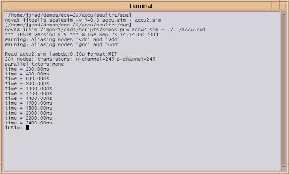
There is one technical detail. The sim file we just created is on a micro-meter grid and not a lambda-based grid. That will cause problems with irsim, which expects a lambda-based design. Use the following command to create the file “accu2.sim” from the original “accu.sim” netlist:
osucells_scalesim –v l=0.3 accu.sim > accu2.sim
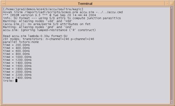
We set lambda to 0.3, which is the correct value for the AMI 0.5um technology. The output will be called accu2.sim. Now we can perform IRSIM simulation using the following command:
irsim /import/app1/scripts/scmos.prm accu2.sim -../../accu.cmd
Note that we placed “accu.cmd” in the same folder as the RTL code “accu.v”. Since this is two folders above the current directory we used “../” twice. The screen should now look as follows:
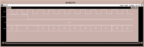
And the graphical waveform output will look as follows: We see that the accumulator still behaves as expected. At every rising clock edge the value of “in” is added to the accumulated value.
We now have a verified sim netlist that we can compare against the layout for LVS verification.
7) Layout-Versus-Schematic (LVS) Verification
At this point we are ready to verify the mask-level layout we created with Silicon Ensemble. It was created in the folder “magic” in the folder “seultra”. If you are still in the “sue” folder you will have to leave that folder first. Open the magic layout as follows:
cd ..
cd magic
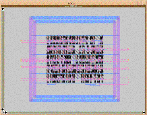
magic accu
The layout will look similar to the following screen. Silicon Ensemble placed all the gates in five rows. Since the routing density is highest in the center, there are some gaps to provide more tracks for the router. The inputs and outputs are created on the left and right edges of the layout. Finally, supply rings for VDD and GND surround the layout.
To extract the layout do the following:
:ext
Now we can exit magic. Be sure to save the complete layout using the “write” command:
:write force
:q
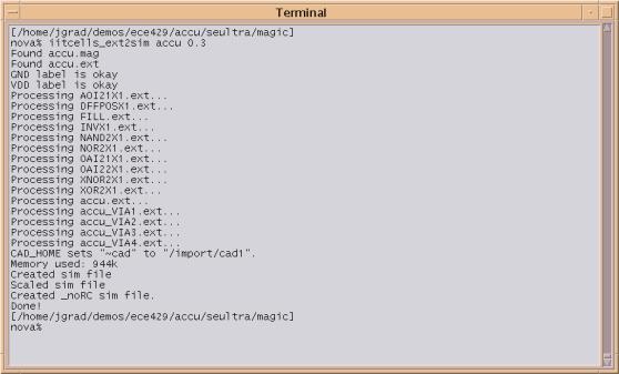
We will need two different sim files. One that includes parasitic elements so we can perform accurate IRSIM simulations. But we also need a sim file without parasitic elements for LVS. Use the script “osucells_ext2sim” to easily create both files in one step. As an added bonus, this command will also ensure that both sim files are on the lambda-grid. Sometimes Silicon Ensemble has to lay down wires on the half-lambda grid, which “osucells_ext2sim” will correct for us.
The command line is as follows:
osucells_ext2sim accu 0.3
We specify that our Magic layout is called “accu” and that our desired value of lambda is “0.3”, just as we used for the schematic. The screen will look as follows:
We now have two sim files:
- accu_noRC.sim Sim file without parasitics (for LVS)
- accu.sim Sim file with parasitics (for IRSIM)
To perform LVS, use the following command:
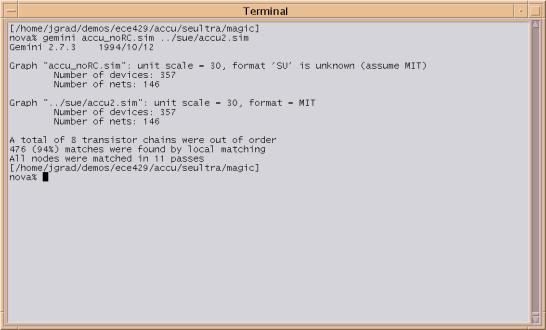
gemini accu_noRC.sim ../sue/accu2.sim
Note that the Sue schematic is located in the folder “sue”, which is on the same level as the current folder. We use “../” to access the folder above the current one and then “sue” to access the folder where the Sue layout is located.
The output from LVS will look similar to the following screen. Ignore the message “A total of 8 transistor chains were out of order”. We are interested in the final line, which reads “All nodes were matched in 11 passes”. This means that the Layout and the Schematic are identical. Therefore, Silicon Ensemble created a layout that is identical to the gate-level netlist. If that were not the case then Gemini would not issue the “All nodes were matched” message.
8) Layout Simulation
At this point we are fairly confident that our layout is correct, since it matches the schematic. And the schematic has simulated successfully in IRSIM and was derived from the gate-level netlist. But still, there are many factors that influence a design on the mask level. It is very important to simulate at least a couple of test vectors. Typically they would be chosen to excite the critical path in the circuit. That would allow conclusions about the speed of the circuit, which can now be measured very accurately since we now have the full mask level representation. Again, note that we get a very detailed number, but since we are at such a low level of abstraction, it would be very time intensive to go back to a higher level if we were to find out that timing is not met.
To run irsim, use the following command line
irsim /import/app1/scripts/scmos.prm accu.sim -../../accu.cmd
The screen will look similar to this:
The waveform window is not shown here as it should be identical to the one obtained from the schematic simulation.
9) Printing the Layout
At this point we are ready to print the layout for the lab report. We will create a postscript or .ps file, which is a common graphics format under Unix. You can use Acrobat Distiller which can be found on most PCs to create a PDF file.
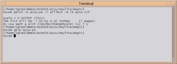
The tool we will be using is called “pplot”. It is able to create a ps file from a cif file. The cif file we can obtain from Magic by using the “:cif” command. The command sequence is as follows:
magic accu
:cif
:q
pplot –k accu.ps –l allText –d 10 accu.cif
gzip accu.ps
The option “-l allText” will remove all text labels from the plot. This is helpful in preventing the layout from being cluttered with text. The output will be written to “accu.ps”. Finally, we use the tool gzip to compress the file. We do this because .ps files tend to be large in size but can usually be compressed by over 90%. You can use any PC de-compress utility, such as WinZip to extract the original ps file.
There are several ways to transport the plot from the Unix network to a PC. The easiest is by using a web browser. On a PC, open the website
ftp://your_unix_account@ftp.ece.iit.edu
Now you will be able to browse the files in your account and download anything you want to your PC.
Since all the files we created tend to be large, always check your disk-space quota. Once you exceed it your account will be locked and files will be deleted. To check your quota, use the command
quota –v
To see how much space a particular project occupies, do
du –ks /home/your_unix_account/your_project
10) Appendix: accu.v
// A simple 8-bit accumulator
// reset=0 -> set acc to 0
// reset=1 -> add "in" to acc
//
//
// Johannes Grad
// gradjoh@iit.edu
//
//
// The core
//
module accu(in, acc, clk, reset);
input [7:0] in;
input clk, reset;
output [7:0] acc;
reg [7:0] acc;
always @(posedge clk)
begin
if (reset) acc<=0;
else acc<=acc+in;
end
endmodule
11) Appendix: accu_test.v
module stimulus;
reg clk, reset;
reg [7:0] in;
wire [7:0] out;
accu accu1(in, out, clk, reset);
initial
begin
clk = 1'b0;
forever begin #5 clk = ~clk;
$display("At Time: %d Accumulator Output=%d",$time,out); end
end
initial
begin
$shm_open("shm.db",1); // Opens a waveform database
$shm_probe("AS"); // Saves all signals to database
#50 $finish;
#100 $shm_close(); // Closes the waveform database
end
// Stimulate the Input Signals
initial
begin
#0 reset<=1;
in<=1;
#5 reset<=0;
end
endmodule // stimulus
12) Appendix: accu.cmd
stepsize 100
vector acc acc[7] acc[6] acc[5] acc[4] acc[3] acc[2] acc[1] acc[0]
vector in in[7] in[6] in[5] in[4] in[3] in[2] in[1] in[0]
clock clk 1 0
ana clk reset in acc
set in 00000001
h reset
c
c
l reset
c
c
c
c
c
c
c
c
c
c